|
Part 2: CPU & ROM Testing |
|
|
ROM_eaea.asm Address & Data Buses Capture
Start of .bin file End of .bin file
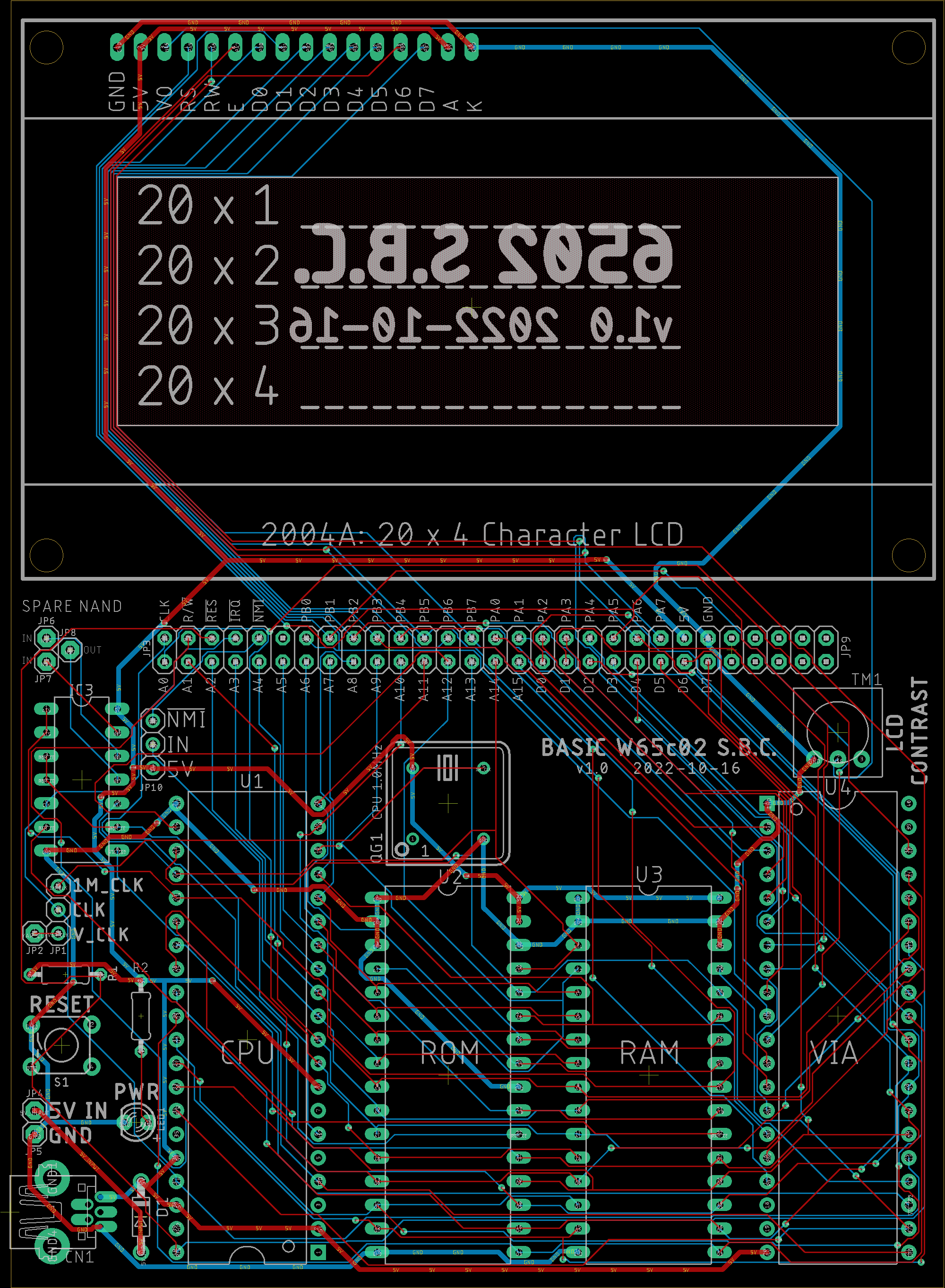
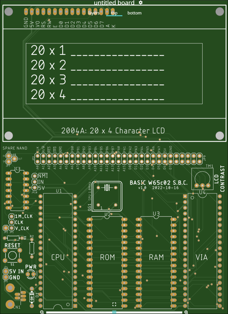
Eagle: Schematic Eagle: Board Layout Gerber Viewer: PCB Layout
|
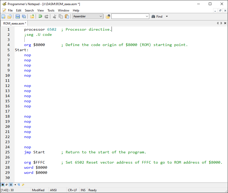
After removing the 8 resistors from the data bus that have been arranged in an 0xEA hex pattern, I programmed the ROM with code that would cause the system to behave in the same manner as the resistors. The code is ROM_eaea.asm which you'll find zipped up so your antivirus software doesn't get "bent out of shape". You can click on the first (left) screenshot to to see it.
The second (right) screenshot shows the contents of the address and data buses captured by the Arduino Mega 2560. The top yellow highlights show the Reset Vector address read of 0xFFFC and 0xFFFD for the value $8000 which causes the Program Counter to go to that position in the next captured line. There it reads 0xEA - the NOP instruction - which is what was configured at the top of the "Start:" section of the ROM_eaea.asm file.
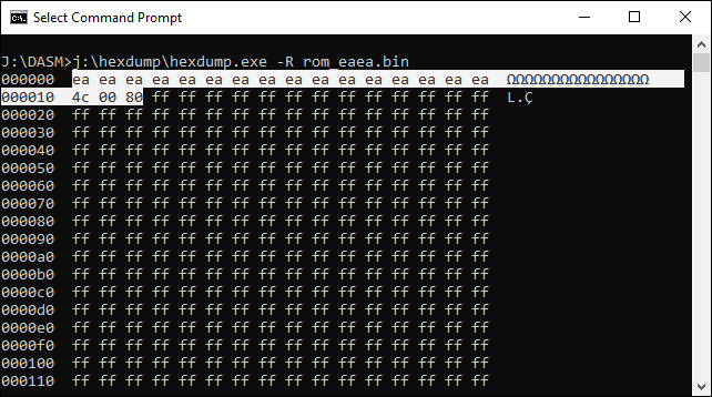
The next two screenshots show the assembled code that will be burned to the EEPROM.
In the third screenshot, the first 16 bytes show the 0xEA pattern followed by 0x4C (jmp) and the 0x8000 address to jump to. The rest of the code is 0xFF which is the default for the MiniPro EEPROM programmer.
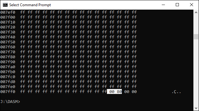
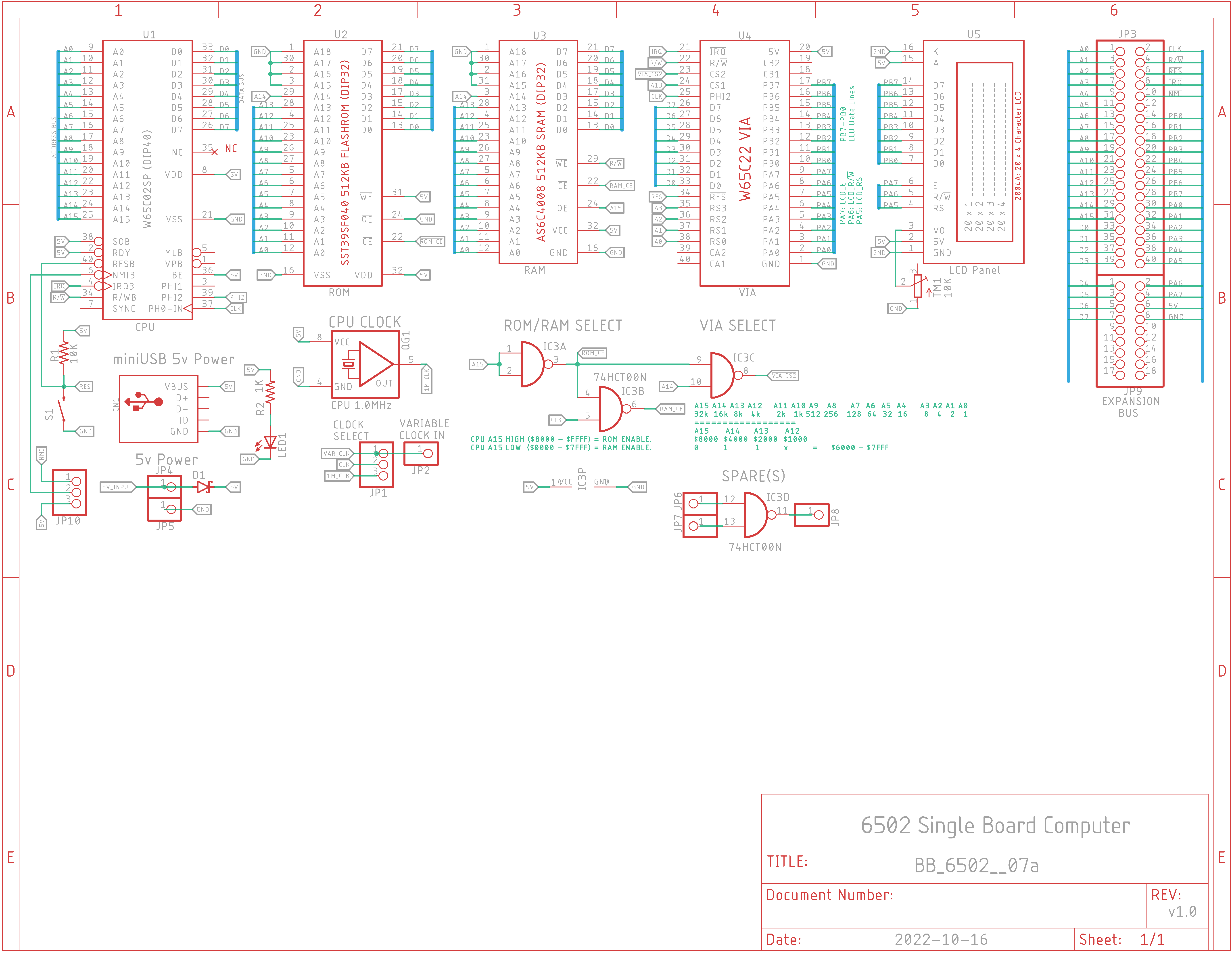
In the fourth screenshot you'll see the value 0x8000 found at locations 0xFFD and 0xFFFC which is the Reset Vector address for the 6502. This is the location the 6502 will put into the Program Counter Register to start our system's operation. You'll notice the address shown is not 0xFFFC but 0x7FFC instead. That is because the ROM has been selected as the high address range of $8000-$FFFF using the ROM_CE signal but the ROM address locations start at 0 and go to $7FFF, not $8000. When the CPU outputs address $8000 onto the address bus, pin A15 is asserted high. When that signal travels through the NAND gate IC3A, it is inverted to a low which enables the ROM's CE pin. So any address in the upper range ($8000-$FFFF) will be handled by the ROM, not the RAM.
The CPU is now able to read the simple code in the ROM so we know both the CPU and ROM are "good to go".
The next tests will be for the RAM and VIA.
|