|
Part 4: VIA & LCD Testing |
|
|
LCD Wired to VIA 2004A LCD Instructions
DDRAM Address Instruction DDRAM Address Position
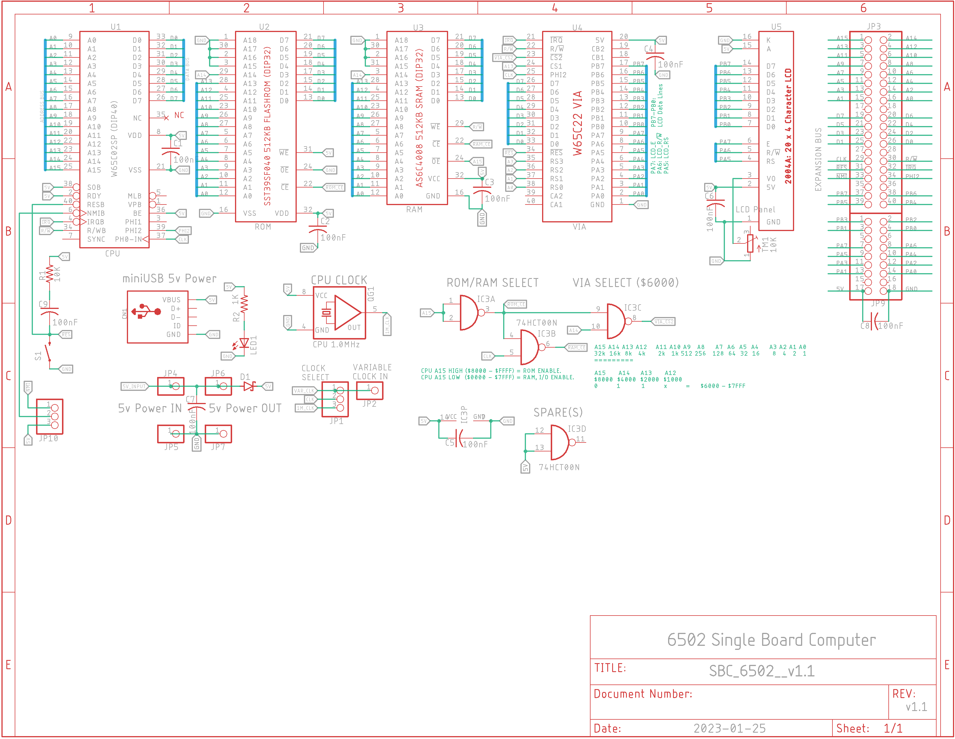
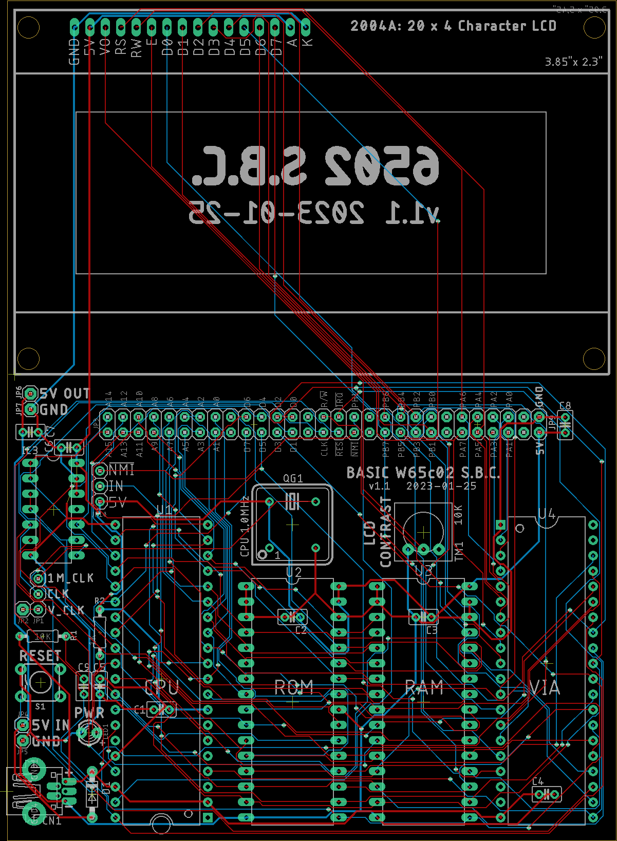
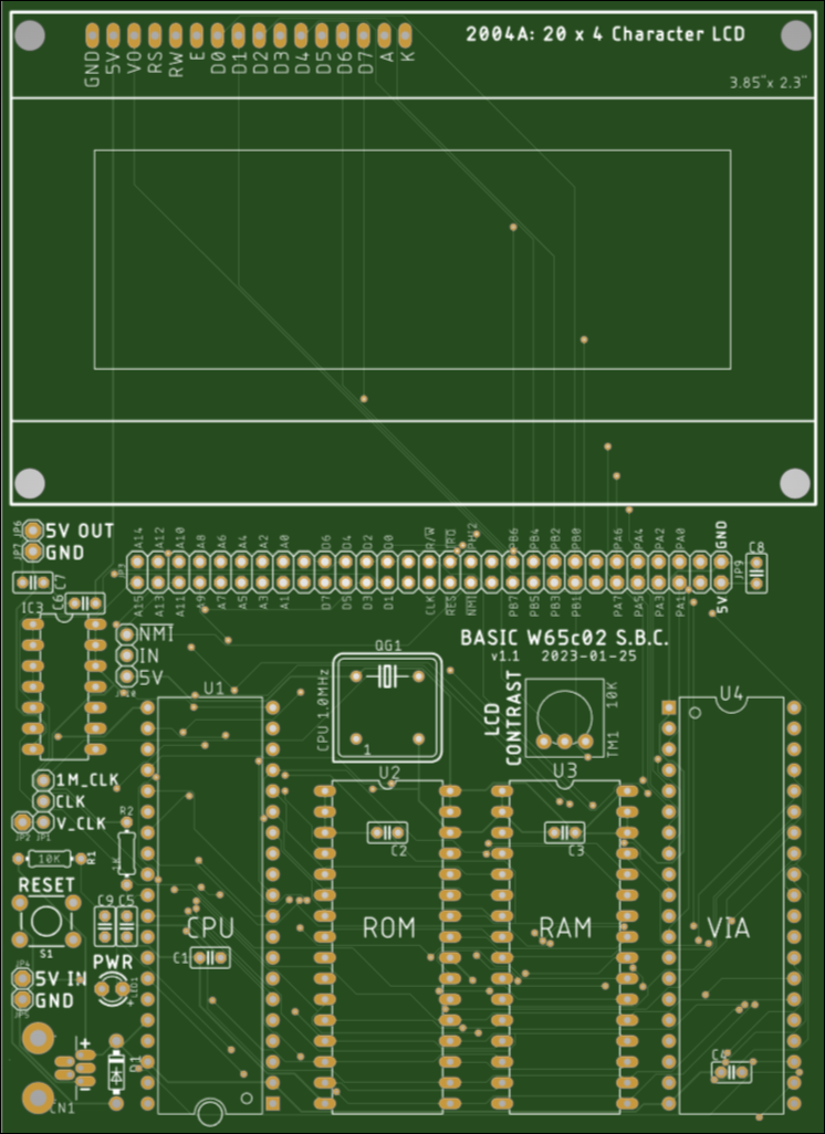
v1.1 Schematic v1.1 Board Layout v1.1 PCB Layout
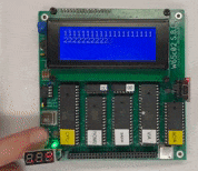
Video: VIA-LCD Code Execution at $6000 on v1.0 SBC and v1.1A SBC
Left Video: To the left of the v1.1 SBC is the clock generator running in Astable mode at about 500Hz. Below the SBC is an Arduino Mega2560 clone that is acting as a Logic Analyzer. It will display all of the bits and bytes seen on the bus to Arduino IDE's serial monitor. Right Video: the v1.1A SBC has an onboard variable clock generator and an ACIA UART.
v1.0 PCBs work well. v1.1A PCBs work even better
|
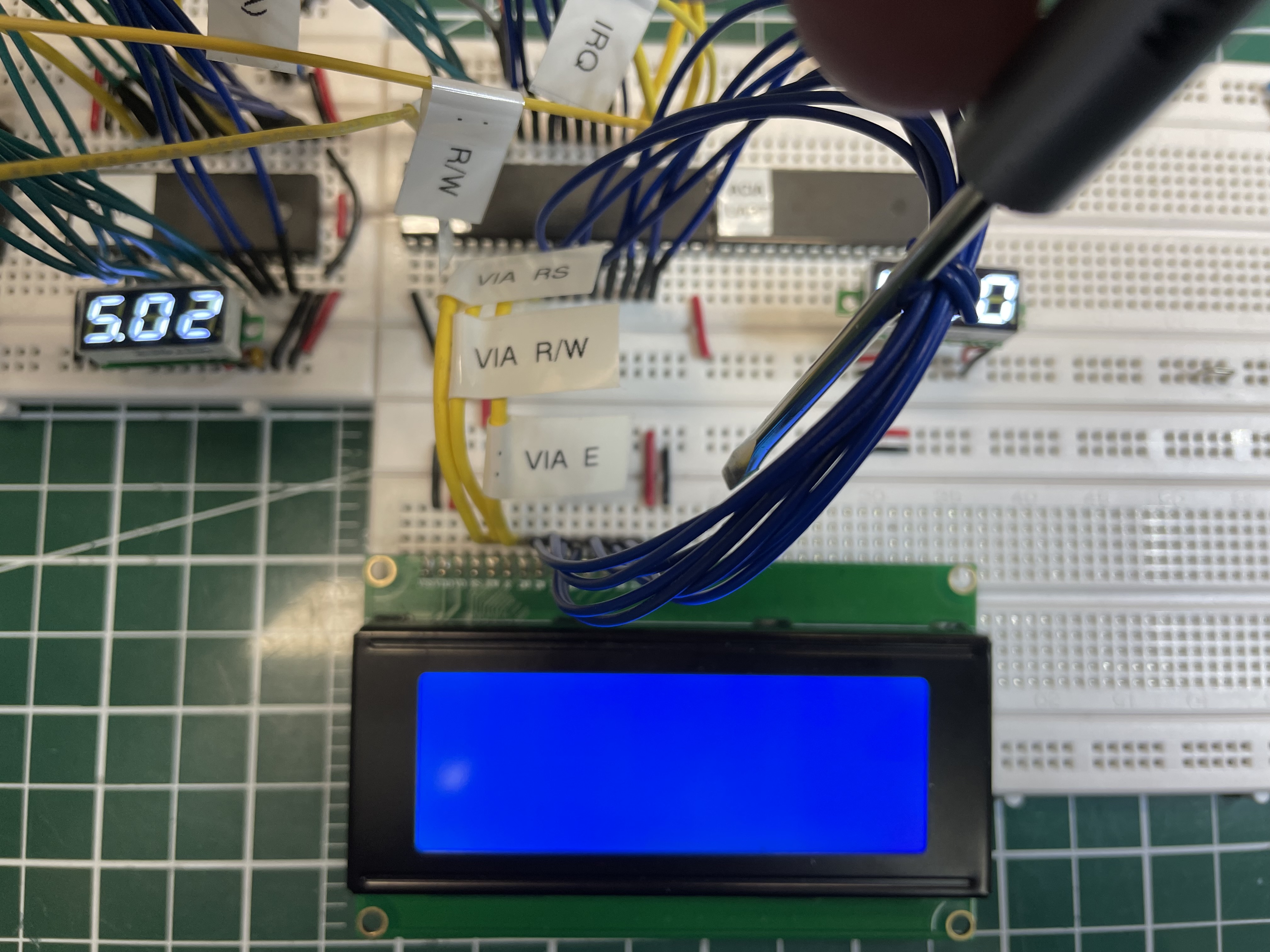
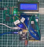
Implementing the WD65c51 VIA with an LCD Panel We know the VIA works well so we'll attach a "4 rows of 20 characters" LCD panel to it. It is commonly known as a 2004A.
Testing the LCD We hooked up the 2004A LCD to the VIA as per the schematic and wired in a 10K pot to the VO pin to adjust the LCD display's contrast.
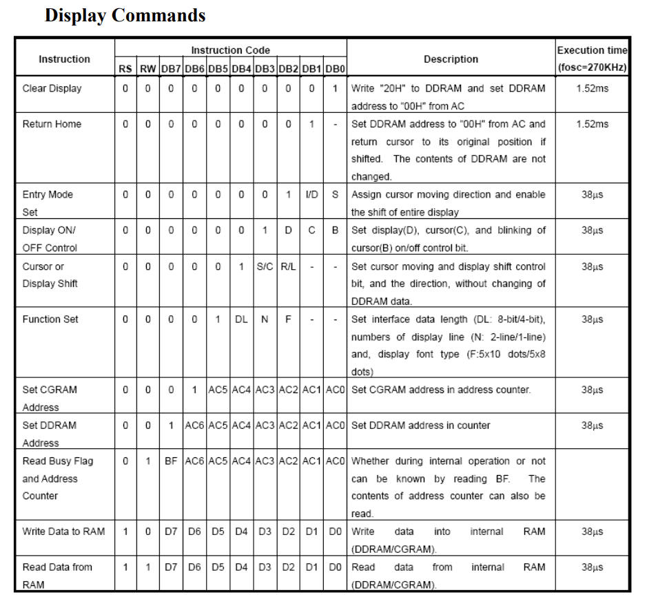
Here is the manual for the original Hitachi 16x2 LCD panel: HD44780U LCD-II. Most other LCD displays are a variation of this one. The programming codes are mostly the same; LCD instructions can also be found here.
The schematic and board have been modified to include the LCD panel. As you can see in the green PCB Layout screenshot, the LCD is at the top and the 6502 computer is at the bottom.
If you watched at least the first 9 Ben Eater 6502 videos, you'll recognize this assembly language program VIA_LCD_4_0x6000.asm which is a variation on Ben's. It displays numbers across all 4 rows of the LCD display.
The 2004A LCD's behaviour is a little unusual which required changing the code to suit. The original Hitachi display was two lines of 8 characters, or 8 x2 as it's known. This matured to 16 x 2 and finally 20 x 4 (2004A) which is what we're working with today.
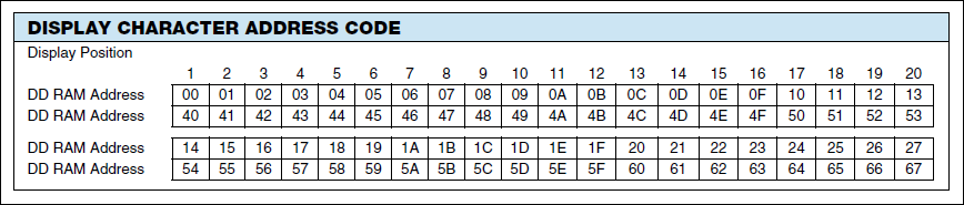
The LCD assumes that 40 characters will be used on two rows for a total of 80 characters... or more. We can name the rows A and B. For the first row, row A, 20 characters go on line 1 of the display and the remaining 20 go on line 3. For the second row, row B, the first 20 are on line 2 and the remaining 20 are on line 4. However, the numbering scheme is a little weird. If you click to expand the adjacent thumbnail, DDRAM ADDRESS POSITION, you'll see that the numbering of the first line (0x00 to 0x13) wraps on the 3rd line (0x14 to 0x27). The second line (0x40 to 0x53) does not start where the third line left off at 0x27; we expected 0x28 but find 0x40 here instead. This suggests that each row is not limited to 0x27 characters but instead could actually accommodate 0x3F (63) characters if someone were to design an LCD panel to do so. Your reference for the Display Character Address Code is Vishay LCD020n004l.pdf
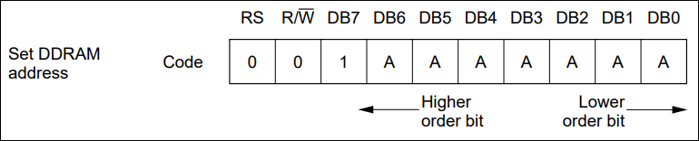
How to get around this weirdness? One way is to use the 0x80 instruction to tell the panel you're going to use DDRAM addressing and then append the address of the first character of your message.
If we were to give the LCD panel 80 characters to display at one time (that's how big its buffer is), they would display on the 20-character by 4-line display as follows: Line 1: Characters 00 to 19 ; 0x00 to 0x13 Line 2: Characters 40 to 59 ; 0x40 to 0x53 Line 3: Characters 20 to 39 ; 0x14 to 0x27 Line 4: Characters 60 to 79 ; 0x54 to 0x67
For line 1, the position is 0x00 so if we add the command 0x80 to it, we would get 0x80. For line 2, the position is 0x28 (it's the start of the second string of 40 characters in the buffer) so if we add the command 0x80 to 0x28, we would get 0xA8. For line 3, the position is 0x14 and adding 0x80 gives us 0x94. For line 4, the position is 0x3c plus 0x80 for a total of 0xBC.
The short video shows execution of the VIA_LCD_4_0x6000.asm to display data on all 4 lines.
|