![]()
|
Voltage Level Shifter
|
||
|
Pix/Vids/Schematics (click to enlarge) |
Info | |
|
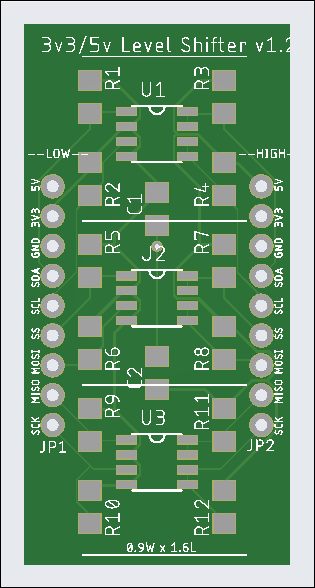
PCB v1.2 Front PCB v1.2 Back
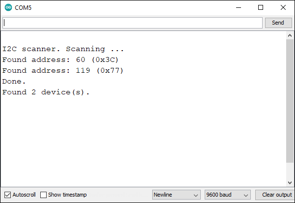
Arduino Serial Monitor shows I2C address scan of BME280 sensor and 0.96" SSD1306 Display
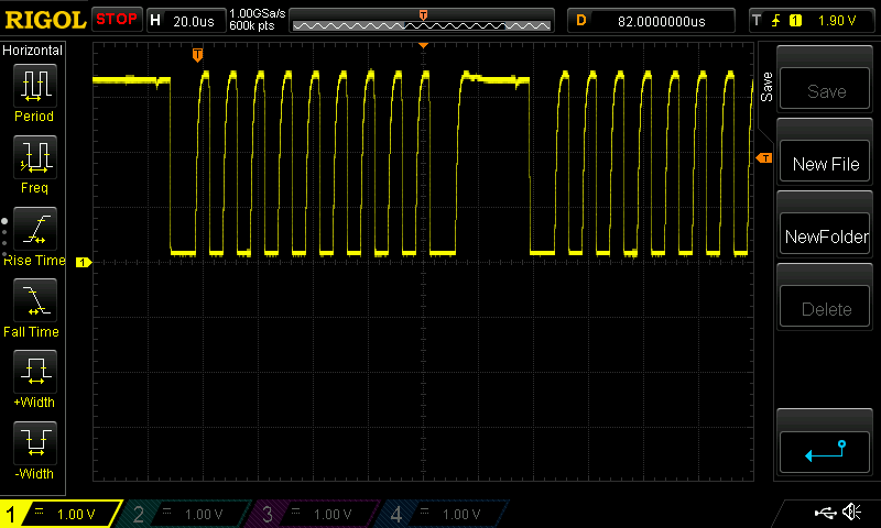
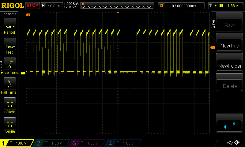
O'scope display of I2C (left) and SPI (right) signals
===================================
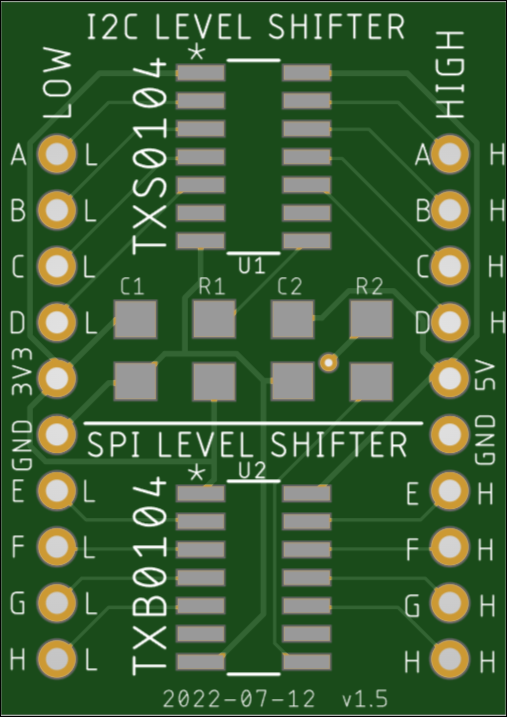
PCB v1.5
|
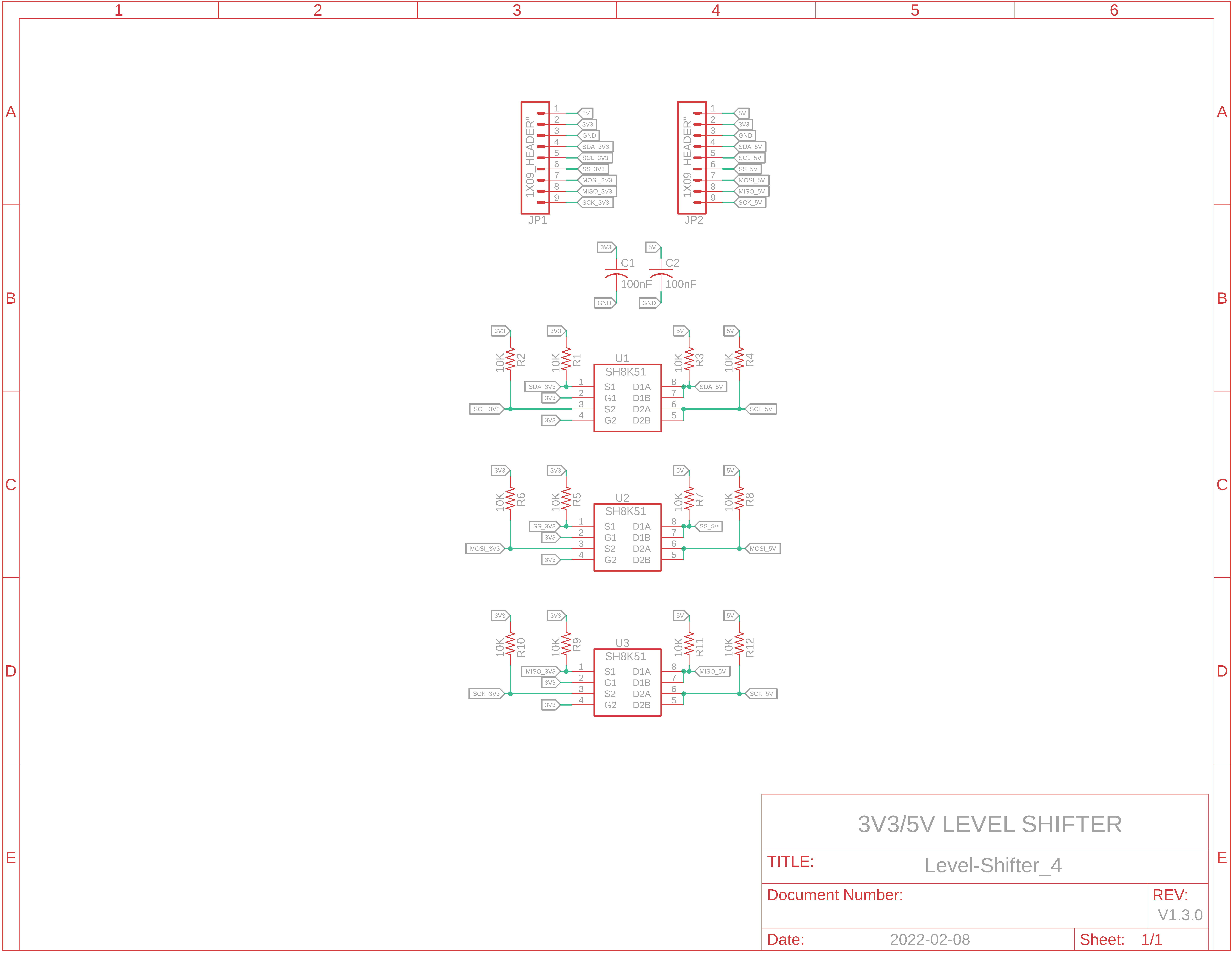
Eagle CAD Drawing v1.3
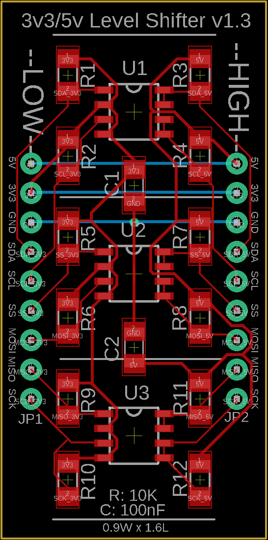
Eagle CAD PCB Layout v1.3
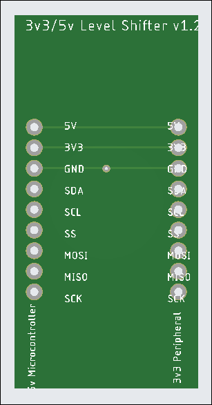
PCB v1.3 Hookup
Eagle CAD: v1.3 Bill of Materials
===================================
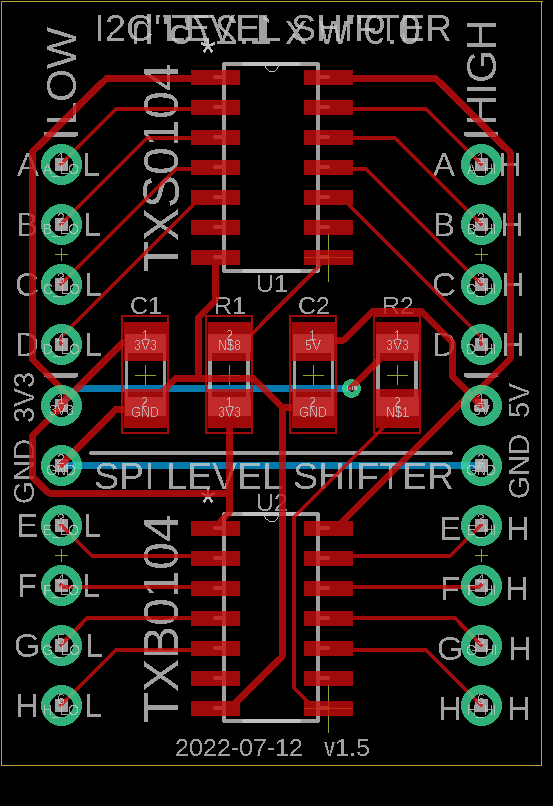
Eagle CAD Drawing v1.5
Eagle CAD PCB Layout v1.5
Eagle CAD: v1.5 Bill of Materials
|
Description: This voltage level shifter allows you to use modern 3.3v peripherals with older 5v microcontrollers. Actually, the voltage choices are up to you and are only limited by either the SH8K51 MOSFET in the v1.3 design or the TI TXS0104 chips in the v1.4 design. v1.2 of the level-shifter has 10K pull-up resistors for both input and output signals as well as decoupling caps for both voltage sources. v1.3 has the silkscreen cleaned up. v1.4 has 10K pull-up resistors built into the chip because it's specifically designed for open-collector I2C circuits.
Details: - Plug the level-shifter board into the center of your breadboard (BB) - Wire the 3v3 pin to one BB rail, the 5v pin to another rail and the GND pin to a common ground - Usage Example: A-HI on the HIGH side connects to SDA from the 5v Uno or Nano, and A-LO on the LOW side connects to SDA on the 3v3 peripheral like an SSD1306 1.3" OLED display - Two I2C pins or four SPI pin connections are possible with one board - These are voltage level shifter and can be used with most digital signals, not just I2C and SPI
Note: If you would rather not use the TXS0104 (I2C) but would prefer the TXB0104 (SPI, etc.), the 14-pin chips are pin-for-pin swappable.
References: Phillips app note AN97055: bi-directional level shifter for I2C-bus and other systems. Texas Instruments also has a guide on level shifters.
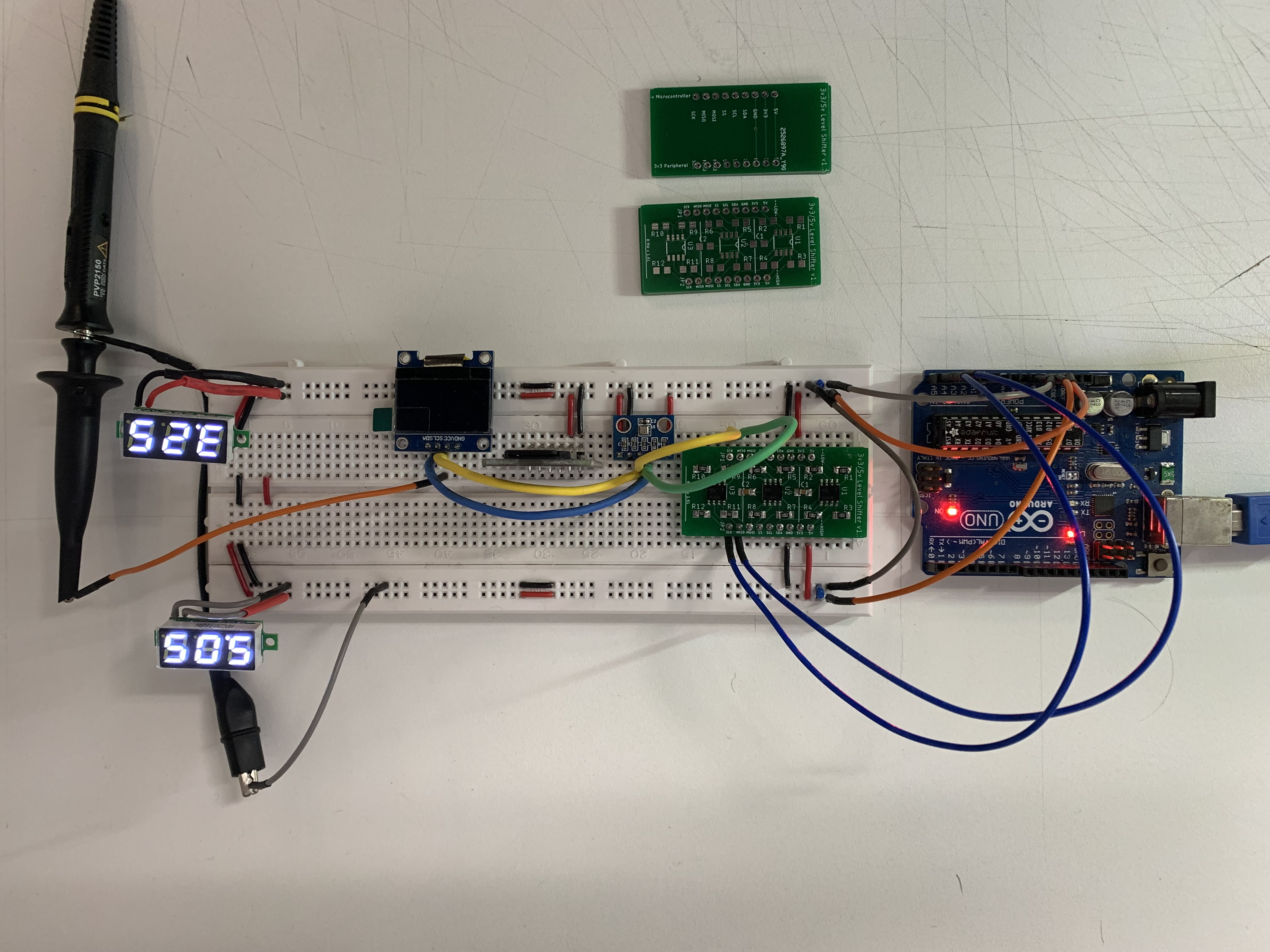
Left Panel Pix: In the left panel you can see pix of the PCB that was sent out for manufacture. The PCBs returned, were populated, defluxed and tested with I2C-Scanner.ino and SPI_SD_ListFiles.ino. The results of the I2C Scanner program show the I2C addresses of the BME280 sensor and the 0.96" SSD1306 display. Below the PCB and Serial Monitor pix are 2 screenshots from my Rigol oscilloscope. The signals from the two I2C and 4 SPI pins (connected to a microSD device) look pretty good without too much signal ringing or overshoot.
Middle Panel Pix: The lower picture of the three shows a 5v Arduino UNO powering the upper breadboard 5v power rail as well as 3v3 to the lower rail. 5v I2C signals, SCL and SDA, are provided to the upper part of the Level Shifter (LS). The signals go through the LS to the lower part and are output as 3v3 signals which are attached to the tiny SSD1306 128x64 0.9" OLED display, which is daisy-chained to the BME280 sensor.
PCB v1.5 I2C: This design uses both the TXS0104 designed for 2-wire I2C circuits and the TXB0104 designed for 4-wire SPI circuits. The I2C chip contains 10K pullup resistors on both low and high side open-drain pins so none were needed for the PCB. Pullups are not needed for the SPI circuit. OE (output enable) is pulled high for auto-direction sensing operation. 100nF decoupling caps were added to both power supply inputs. |

+
Updated 2022-07-12 @ 8am
![]()