|
CIRCUIT 1-6-4: I/O Decode Logic |
| Name | Circuit Schematics (click to enlarge) | Info |
|
I/O Decode Logic
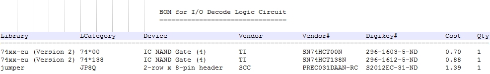
(Bill of Materials)
|
Eagle CAD: I/O Decode Logic
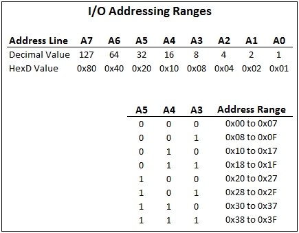
I/O Address Ranges
|
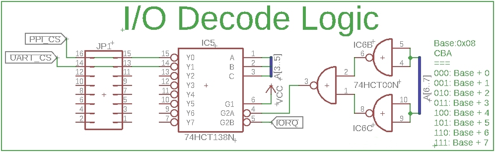
If you examine the decode logic used in the previous schematics above, you'll notice the address bus "feeds" to the 74138 decoder are not sequential. Moving forward in this and subsequent module designs, we're going to change the addressing so it is sequential. A0 to A2 (not shown) will go to the device (PPI or UART) to convey commands or data, A3 to A5 are used for the addressed enable lines, and A6 to A7 are used to enable the '138 decoder itself at pin 4, G2A.
If I/O binary address 0000 0000 is chosen, the '138 decoder is enabled on G2A and inputs A, B, and C. The first enable line output Y0 or pin 15 on the '138 is selected. This enables the PPI used for the keypad and LCD panel. Pins A0, A1, and A2 mean that eight I/O addresses (0x00 to 0x07) will be used to address the specific device; the PPI will only use A0 and A1, that is, addresses 0x00 to 0x03. Because the base address is 0x00, the addresses A0 to A2 addresses, 0x00 to 0x03, are added to the base address of 0x00 to create the final result of addresses 0x00 to 0x03.
If I/O binary address 0000 1000 is chosen, the decoder is enabled on G2A and the second enable line Y1 (pin 14) on the '138 is selected. This enables the UART used for serial FTDI or RS232 communications; we'll build that circuit later. Pins A0, A1, and A2 on the UART will be used, that is, addresses 0x00 to 0x07. Because the base address is now 0x08, the addresses 0x00 to 0x07 are added to 0x08 to create the final addresses of 0x08 to 0x0F. Consult the adjacent table, I/O Address Ranges for clarification.
If we need to add another device, the A4 address line will be 1 and the A3 line will be 0. A4 has a value of 16 or 0x10. Adding address 0x00 to 0x07 (from A0 to A2) to the base address of 0x10 will give us addresses 0x10 to 0x17.
For the next device, both the A3 and A4 lines will be used, thus the base address becomes 24 or 0x18. The full address range for that device will be 0x18 to 0x1F.
As you may have guessed, each addressable device will use a starting address that is a multiple of A3 which has a value of 0x08. |