|
ZB64PC-bus Serial Interface Board |
| PCB Circuit (click to enlarge) | Circuits and Info |
|
Eagle CAD: 1. Arduino Nano Interface
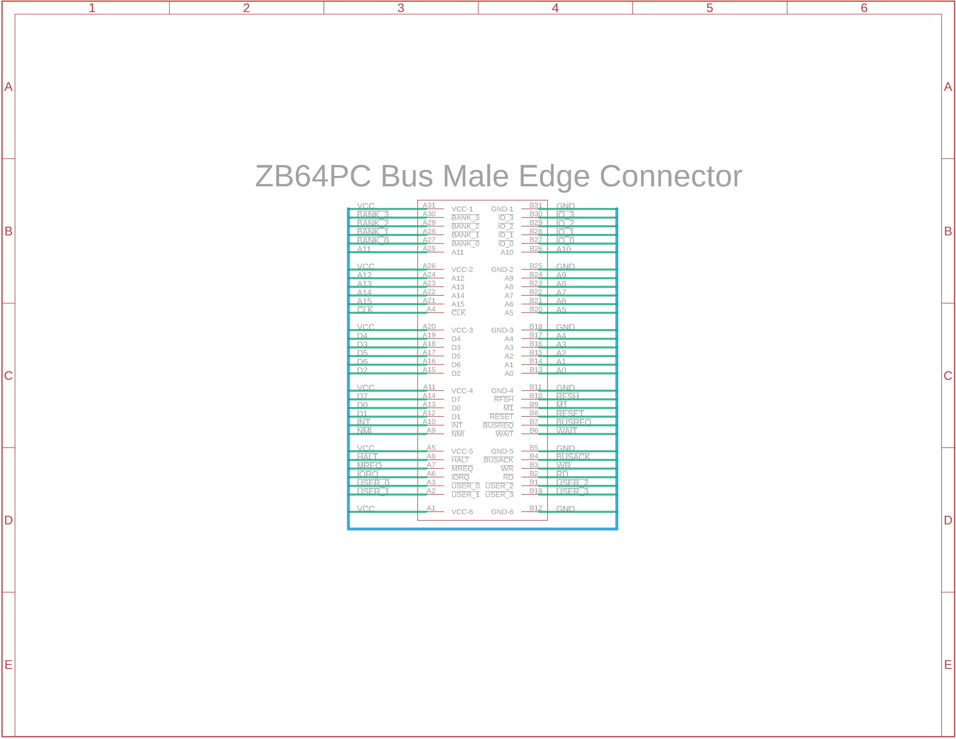
Eagle CAD: 2. M62-bus Male Edge Connector
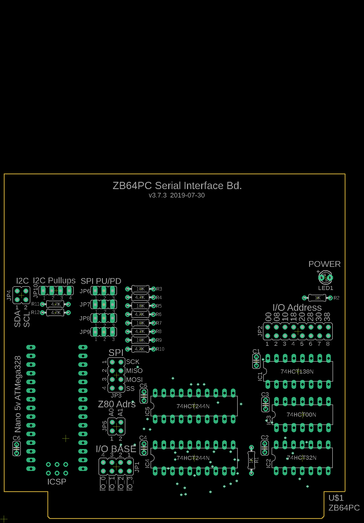
Eagle CAD: 3. A Possible PCB Layout
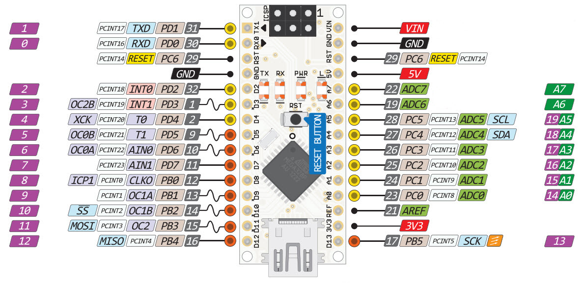
Arduino Nano v3 Pinout
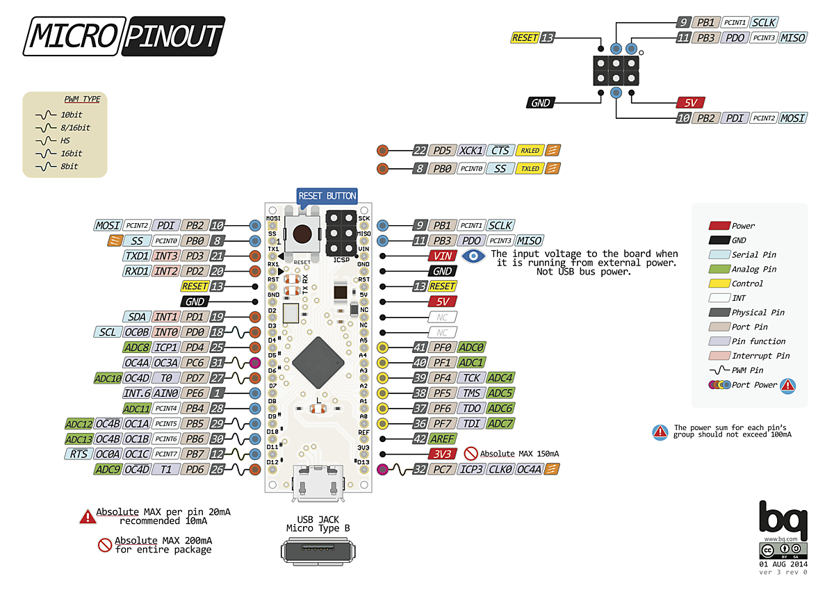
Arduino Micro Pinout
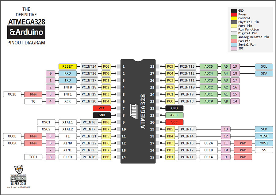
ATMega328 Pinout
(Bill of Materials) |
PLEASE NOTE: I do not sell production boards. If you would like to buy an M62 Z80 system board/parts kit, contact Peter Murray, Peter@39k.ca I simply provide you with information to build your own breadboard computer.
I HAVE NOT TESTED THIS BOARD DESIGN YET. PROCEED WITH CAUTION.
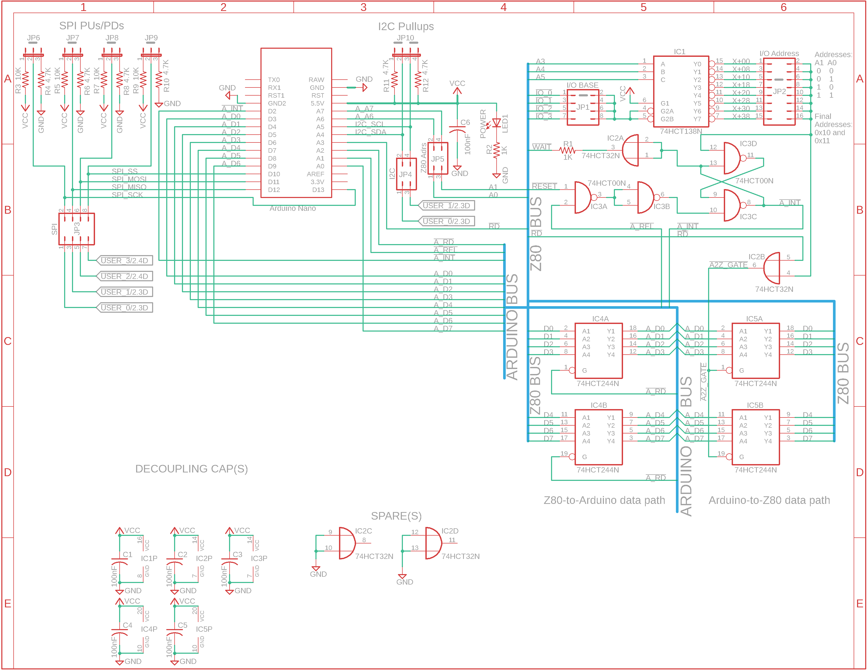
Giving credit where it's due The Serial Interface board was designed by Peter Murray to allow the Z80 to communicate on its 8-bit parallel data bus to a 5v Arduino Nano (or Micro) that you would connect to your I2C and SPI devices like RTC, SD, weather sensor, etc.
Overview If you attempt to use the Z80 and either an 8255 PPI/PIO or a UART to communicate with SPI or I2C devices like a Real Time Clock (RTC) or Barometric/Temperature sensor, you're probably going to have to bit-bang the processor to communicate with these modern modules. One alternative is to let a microcontroller like the Arduino do all the "heavy lifting". Instead of the Z80 sending one bit at a time serially, the uC will send 8 bits in parallel on its Data bus to the Arduino. The microcontroller can be configured in the usual fashion (using C++) to communicate with the serial device.
How does it do it? A Z80 OUT or IN instruction is used to write or read to either a control address or a data address (using A0 and A1).
General operation During a write-to-IO-bus operation, '244 IC4 is enabled to gate the Z80 D0 to D7 signals onto the Arduino bus via the A_RD signal. During a read-from-IO-bus operation, '244 IC5 is enabled to gate the Arduino A_D0 to A_D7 signals onto the Z80 bus via the A2Z_Gate signal; the latter was initiated via the Z80 RD signal. For orderly flow, the WAIT signal to the Z80 is used whenever a Z80 (I/O) OUT or IN instruction for the I/O address range is executed. Normal operation is resumed when the Arduino sees the A_Release signal. The Arduino was initially interrupted via the A_INT signal.
Specific operation In the schematic, the pair of '244s act as a set of direction gates: - IC4 is for the 'Z80 -> Arduino' data path which is enabled with the A_RD line controlled by the Arduino. - IC5 is for 'Arduino -> Z80' data path and is controlled by the gated RD signal A2Z_GATE from the M62 Z80 bus.
The latter is done because we want the data to be
available to the Z80 when it wants to read it from the Arduino but
we can't make the Arduino switch its data lines to high-Z fast
enough when the read is done so as to not interfere with the Z80. - The Z80's OUT/IN command will set the address (and data) bus and trigger the latch via A2Z_GATE - The latch will hold the Z80 in WAIT and trigger the Arduino's INT via A_INT. - The Arduino will read the Z80 RD line to see if we are writing (RD high) to the Arduino or reading (RD low) from it. - If Reading from the Arduino (RD will be low): --- The Arduino will read the 2 address lines (A0 and A1) to determine what port is being written and perform the required action --- The Arduino will set its data bus lines (A_Dx) to be output and latch the appropriate data onto it --- The A_RELEASE will trigger to release the Z80 from its WAIT state --- The Z80's IN command will complete and the data will be read in from the Arduino's data lines via the '244s -
If Writing to Arduino (RD
will be high): --- The Arduino will read the 2 address lines to determine what port we are writing to and perform the required action --- The A_RD will be disabled and the A_RELEASE will trigger to release the Z80 from it's WAIT state
Bus signal lines: Your Z80 can now talk to SPI- or I2C-based devices. We have connected both signal groups (SPI: SCK, MISO, MOSI, SS and I2C: SDA, SCL) via jumpers. JP3 and JP4 would need to be jumpered to support SPI or I2C. I am designing another bus called ZB64EC that uses EuroCard connectors which support 64 connections (the IBMPC 8-bit interface supports 62), of which 12 will be USER configurable signal lines. The USER lines can carry anything you like including SPI and I2C. I'll introduce the new bus after I have tested it extensively which may take a little while because I have to convert all of the existing M62 boards to the new format.
Termination resistors: Both SPI and I2C can be finicky (especially SPI) when it comes to signal terminations needed for master or slave modes. As such, I have provided optional 4.7K pullups for I2C. Additionally, I have provided optional 10K pullups and 4.7K pulldowns for SPI. You can see them labelled in the upper left corner of the schematic as SPI PUs/PDs. Usually, it's only MISO that would need a pullup resistor but I've given you options for all 4 signal lines.
Development space: There is room at the top of the board if you wish to add prototyping pads along with horizontal GND and VCC lines. You can add your RTC, etc., here without having to wire to a breadboard.
Arduino code: ArduinoIF.ino
I see the schematics. Where is the Bill of Materials parts list? The BOM is at the bottom of the adjacent panel.
How big is the Serial Interface board and what will the printed circuit board look like? The PCB measures 100mm x 100mm (4" x 4"). Click the adjacent thumbnail to see a possible parts layout.
Note: M62 Bus is copyrighted by Peter Murray of Murray Electronics, http://www.39k.ca |
![]()