|
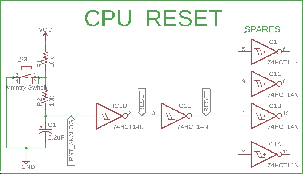
CIRCUIT 1-3: System Reset(s) |
| Name | Circuit Schematics (click to enlarge) | Info |
|
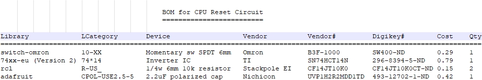
CPU Reset
(Bill of Materials) |
Eagle CAD: CPU Reset Circuit
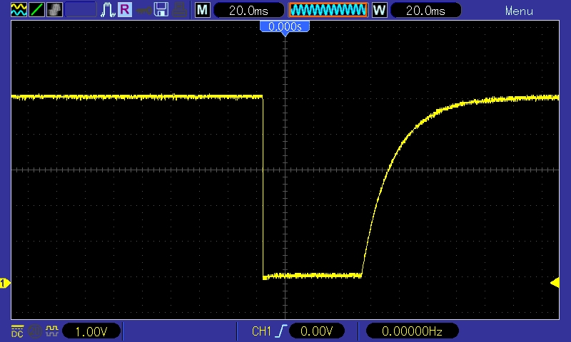
DSO: Analog CPU Reset Signal
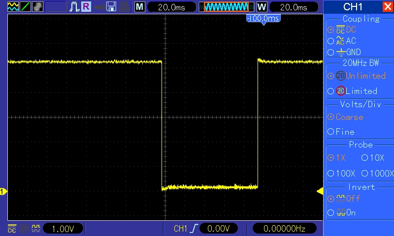
DSO: Digital CPU Reset Signal
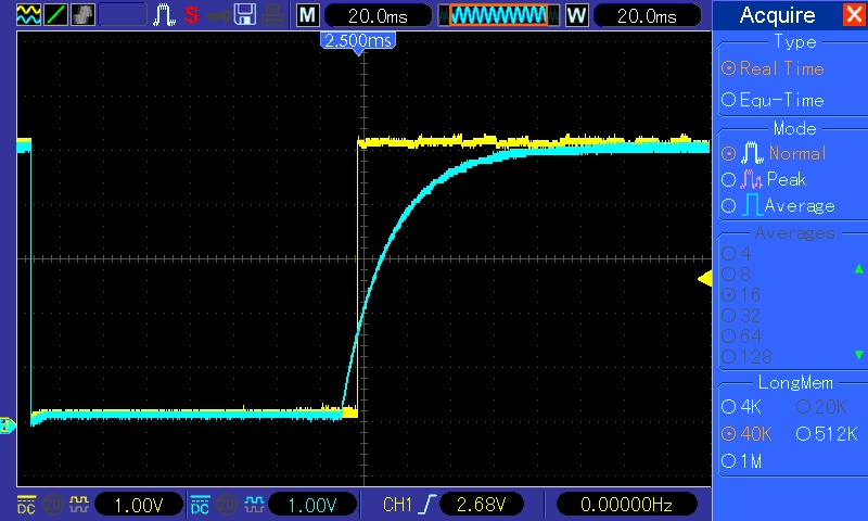
DSO: 2 channels of Analog and Digital
|
In the adjacent schematic, we see an analog reset circuit whose output
is fed to a digital IC. The upper oscilloscope screenshot below the
schematic
was taken where the signal feeds into the IC at RST_ANALOG,
and the middle o'scope screenshot was at the IC exit point called
RESET.
Once the 10K resistor and 2.2uF capacitor in series are fully charged, the signal is held high as "RST_ANALOG" to pin 1 of the 74hct14 inverter IC. The high signal is inverted on the output of pin 2 of the IC as a low which is fed back to the IC's pin 3 where it's inverted again to become a high on pin 4 as the "RESET" signal. You'll need RESET for the Z80 CPU RST and RESET for the 16550 UART for serial communication. Z80 RST is an active-low signal. The output from the inverter`s pin 4 is a logic high signal which is connected to pin 26 of the Z80. It will remain high until the momentary switch is depressed or the circuit is repowered. When switch S3 is pressed momentarily, it pulls the signal from the junction of the resistor/capacitor to ground. We can see that in the o'scope signal in the upper screenshot in the adjacent panel. The signal is long enough (at least 3 CPU clock cycle times) to reset the Z80. The charge time for the RC circuit will be: 10K Ohms x 0.000 002 2 Farads (2.2uF) = 0.022s or 22ms. If the CPU clock is 4MHz, we expect the clock cycle time to be: t = 1/f = 1/4,000,000 = 250ns. 250ns x 3 clock times = 750ns which is substantially less than 22ms so our minimum reset time has been easily met. Using the upper Digital Storage Oscilloscope (DSO) screenshot we can see the natural resistor-capacitor (RC) charge curve. The low, flat part of the signal illustrates the fastest time we could press and release the momentary switch. The curve to the right of the low, flat signal is the RC charge time. If the minimum input high voltage (VIH) is 2V, then we can see it took 3 dots of a 20ms/division display or 12ms of time to reach VIH . Again, this is substantially larger than 0.750ns for a 4MHz Z80 so our reset signal time frame is good. The fact that we are presenting the signal through an HCT version of an inverter, the 74HCT14, presents better compatibility with this older CPU. You can see the output of the 74HCT14 pin 12 to the CPU pin 26 in the middle DSO screenshot. The third DSO screenshot was taken at a later date using 2 channels to contrast the analog reset to the digital reset of a 4MHz signal. TTL high/low reference. |
![]()