|
Z80 Programming VII - Part 1 |
| ROM Monitor: The Hardware |
|
Overview:
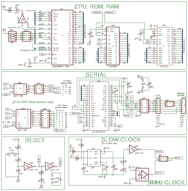
Prior to getting into programming our system to have a ROM Monitor, we'll review the hardware changes. We have changed the Z80 system schematic slightly to give us more control over memory addressing. The schematic for our Single Board Computer (SBC) is adjacent but it's a little hard to read so we've provided thumbnails that will open to larger images in separate browser windows/tabs. Don't forget you can use <CTRL><TAB> to jump between this browser tab and the other tab(s).
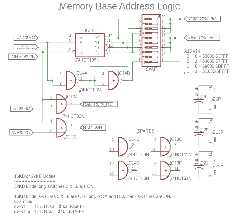
In the first schematic Memory Base Address Logic we have changed the logic to make it more flexible. On the left side, we have added a 74139 2-line-to-4-line decoder. It works the same way the 74138 3-line-to-8-line decoder does. There is a little table to the right of SW1 that shows how address lines A14 and A15 affect it. By using this type of switch, we only enable the appropriate connections. According to the table, if both A14 and A15 are low, we are using BANK_0 and the address for ROM will be $0000-$3FFF (the first 16KB). The upper four switches of SW1 are used to select the ROM address and the next four switches are used to select the RAM address. The upper four are also used to select the memory bank (we'll be building a separate board for memory expansion at a later date). If we enable the switch at pin 1, the ROM will be enabled at $0000. If we also enable the switch at pin 6, the RAM will be enabled at $4000. We can the switches to any unique combinations but we'll have to reassemble our ROM Monitor program ROM-Monitor_DON.asm to match the circuit switches.
Because the '139 uses A14 as its A input on pin 14,
the lowest address is 16KB or $4000, so all address blocks will be
multiples of 16KB, i.e., $0000, $4000, $8000, and $C000. If you are not
going to be building the RAM expansion board, then you have just thrown
away 16KB of ROM and 16KB of RAM of the 32KB chips.
The work around for this is to set all of SW1
switches to OFF, then turn on switches 9 and 10. When A15 is low, pin 9
will be high which is connected the RAM chip select; it will be high so
it will be disabled. Pin 10 however will be low which is connected to
the ROM chip select, thus enabling it. A15 represents 32KB so we'll be
using all of the two memory chips.
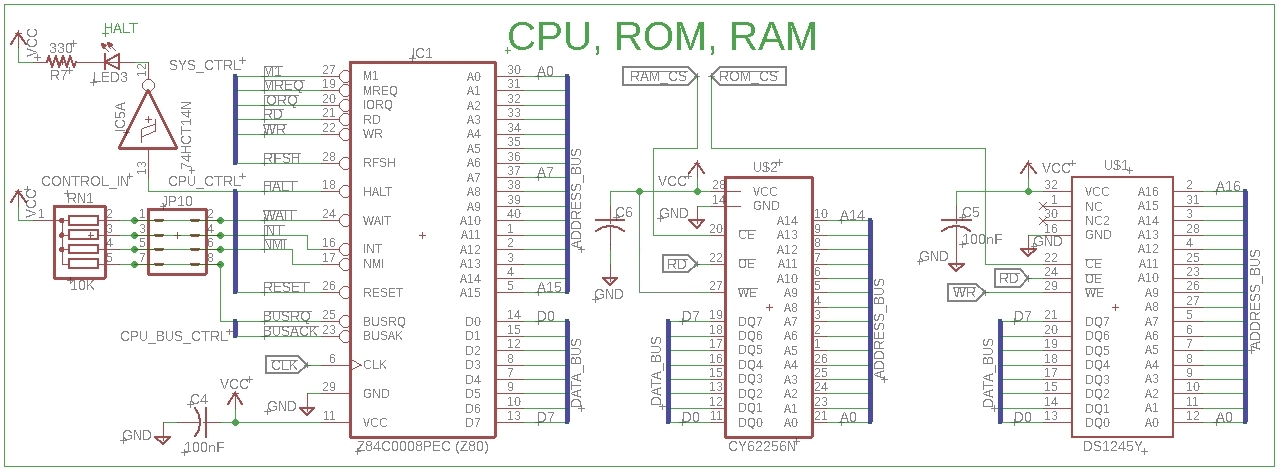
The CPU/ROM/RAM circuit is almost the same as what we have previously used. The HALT signal will now light an LED if the HALT command in code is executed.
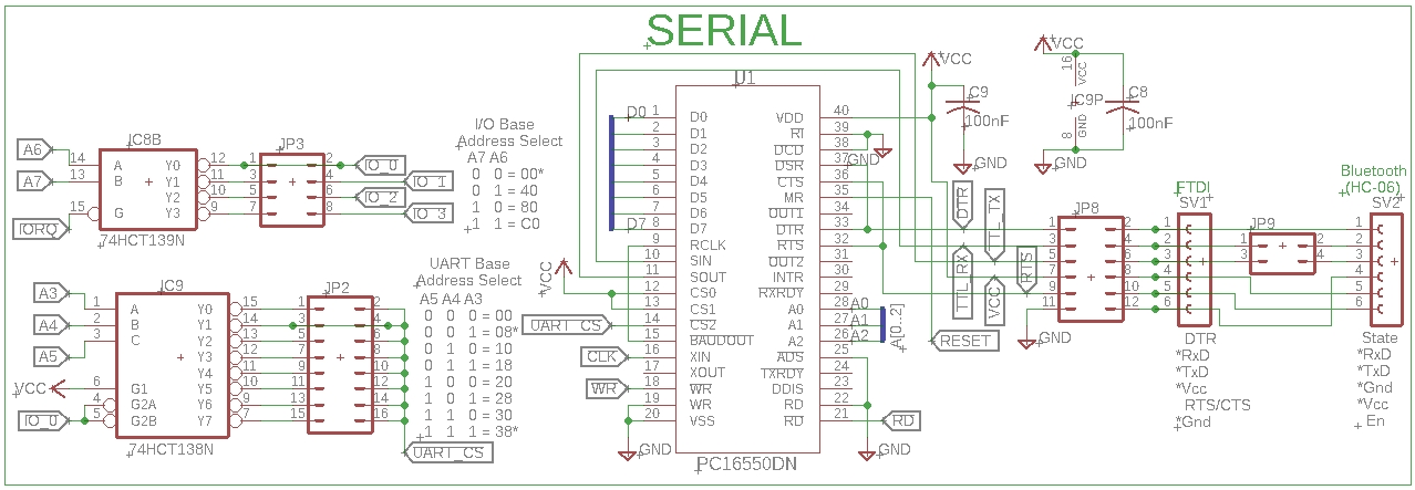
Our TTL SERIAL circuit has changed a little. In addition to adding a 6-pin female strip connector for an HC-06 serial-over-Bluetooth module, we have also adjusted the addressing logic. A 74139 device contains two 2-line-to-4-line decoders and this is the second half; the first half was used for the memory addressing logic. With JP3 pins 1 and 2 jumpered as per the diagram, we will use I/O Base Address Select bank 0 or IO_0. IC9 is a separate '138 used to select the UART_CS signal. Currently, our ROM Monitor uses I/O address $08 with JP2 pins 3 and 4 jumpered. We can easily change that to JP2 pins 15 and 16 jumpered when we change the UART address later to $38.
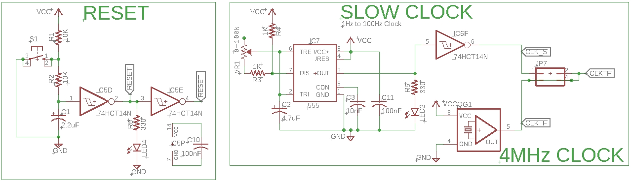
The RESET circuit is the same but the CLOCK circuit has changed slightly. It is now composed of either a slow clock (adjust VR1 potentiometer) that runs from 1Hz to 100Hz, or a much faster fixed speed 4MHz clock. Use JP7 to select which clock will feed the Z80 CPU. For single-stepping, the slow clock would be best.
We'll look at the ROM-Monitor program on the next page. |