|
M62-bus Logic Analyzer Interface Board |
| PCB Circuit (click to enlarge) | Logic Analyzer Interface Board Info |
|
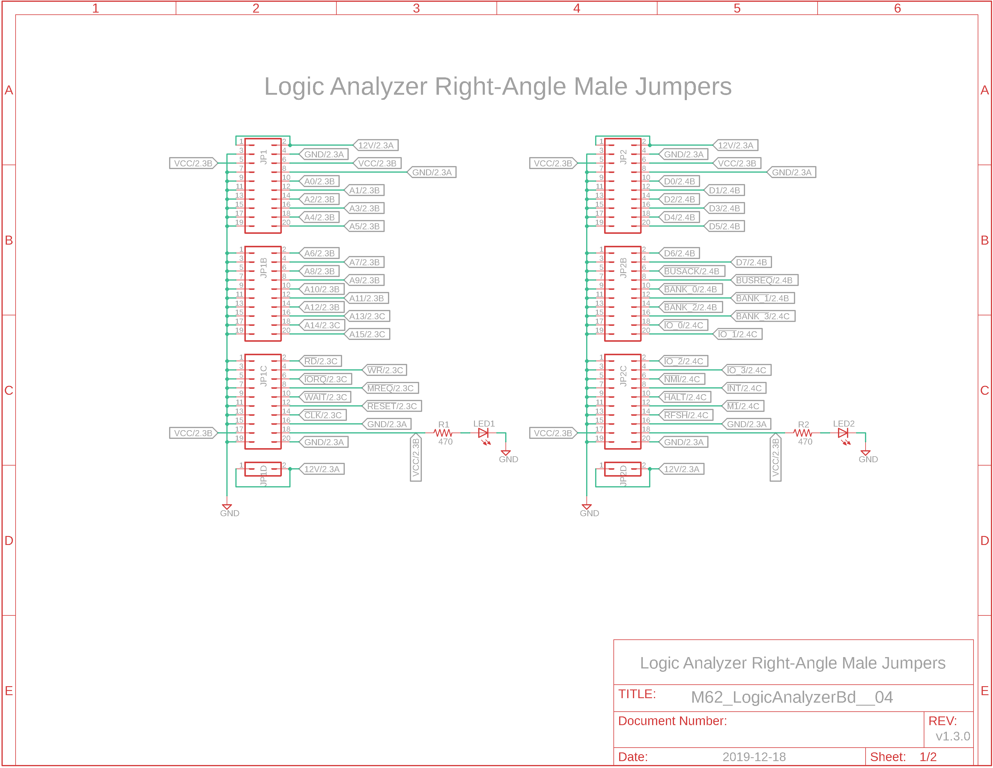
Eagle CAD: 1. M62-bus LA IF Headers
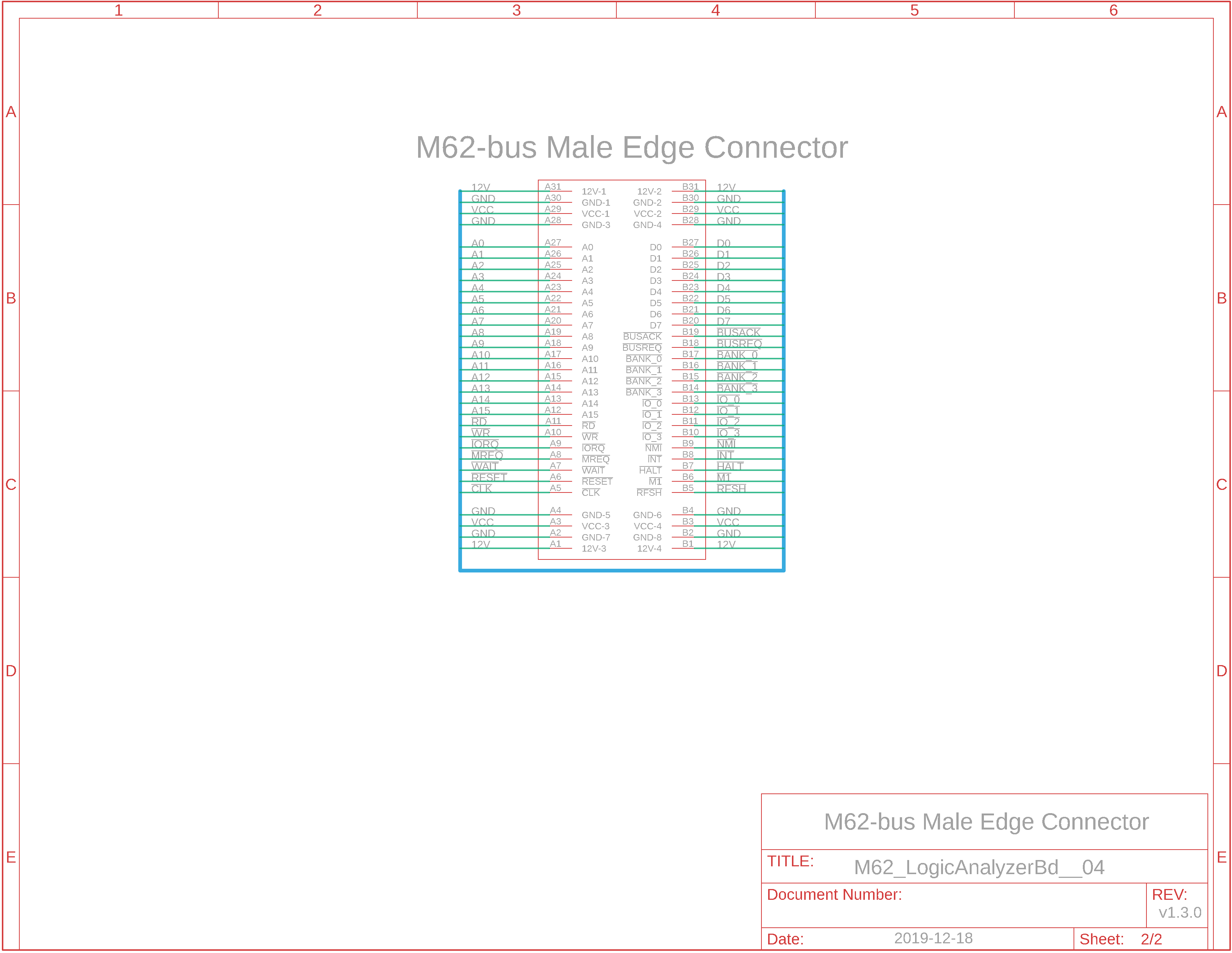
Eagle CAD: 2. M62-bus Male Edge Connector
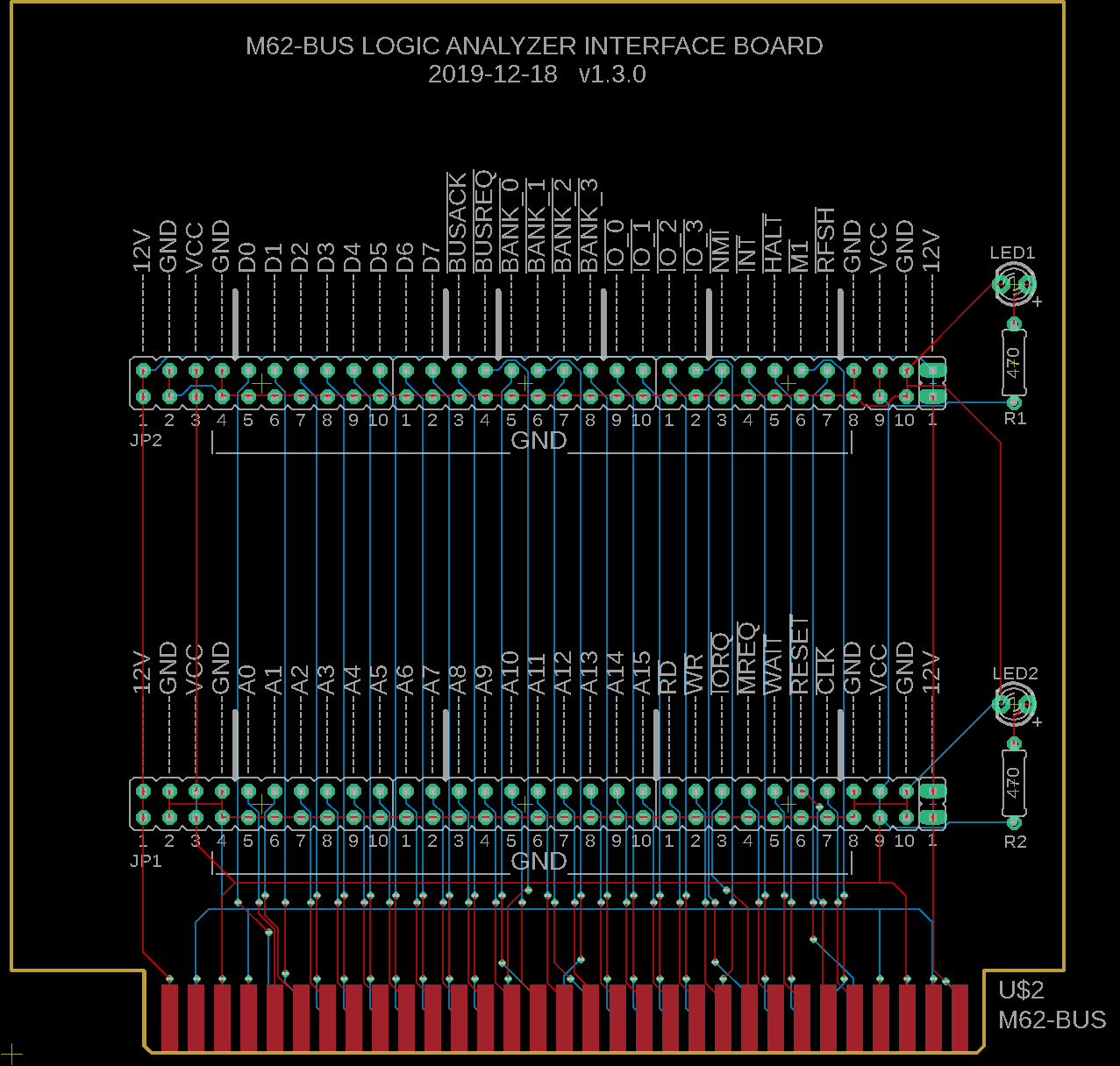
Eagle CAD: 3. A Possible PCB Layout
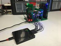
Picture: LA-IF connected to M62-bus
Short MP4 HD Video: Logic Analyzer Interface Bd. capturing CTC board interrupt firing
(Bill of Materials) |
PLEASE NOTE: I do not sell production boards. If you would like to buy an M62 Z80 system board/parts kit, contact Peter Murray, Peter@39k.ca I simply provide you with information to build your own breadboard computer.
NOTE: 2019-12-20 The board files are being sent to China for fabrication. When they return they will be tested thoroughly. For the interim, proceed with caution.
Overview The M62-bus has been duplicated onto a PCB so you can attach a logic analyzer to the bus. All of the Z80 pins as well as the BASE_x and IO_x pins are present and labelled. Each of the signal pins also has a ground pin below it as this seems to be a common feature of the female "flying leads" used by USB-based logic analyzers (LAs) like the DSLogic Plus by Dream Source Lab.
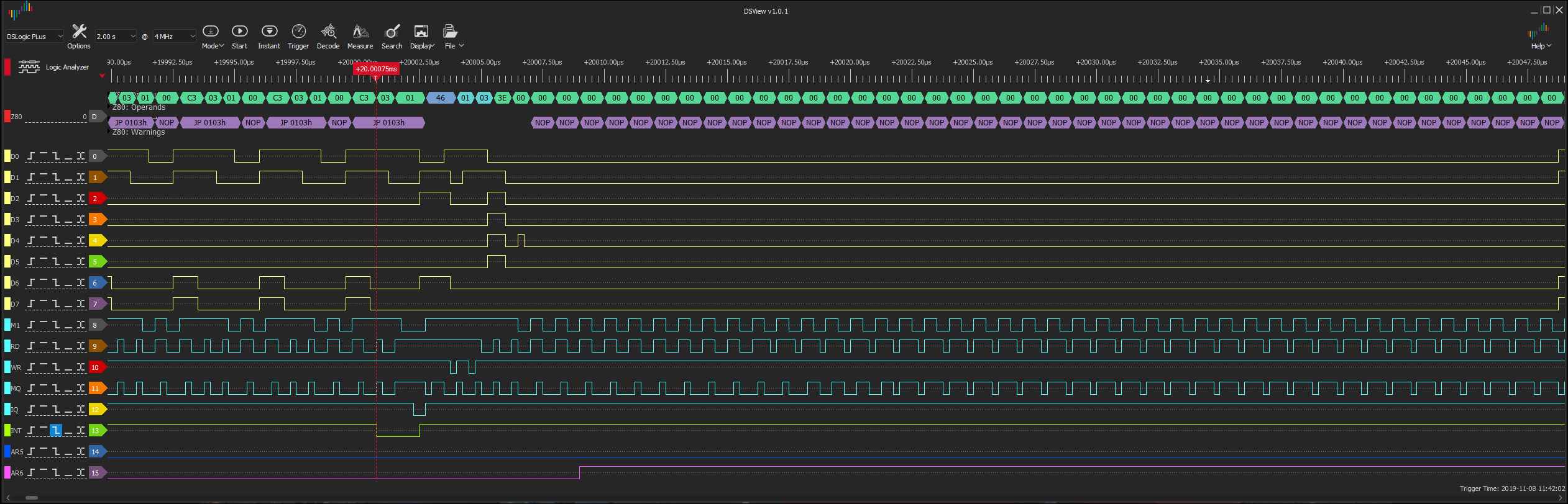
The Logic Analyzer and interface board in operation Three screenshots below show the Logic Analyzer capturing the CTC I/O board counting down and then interrupting the CPU to play a tone/melody on the piezo speaker. The program is running in ROM. See the CTC board section for all kinds of juicy details.
In screenshot
LA_01.png on the left side of
the image in purple text, you can see the repetitive Jumps to
run NOPs. At the red vertical marker line, the
INT
line triggers which causes the interrupt vector register (IVR) value
of 46h to travel on the bus from the CTC to the Z80. While the
CPU is getting its act together, there are a lot of NOPs hence
the reason for the second screenshot, LA_02.png, that shows the
timing further along.
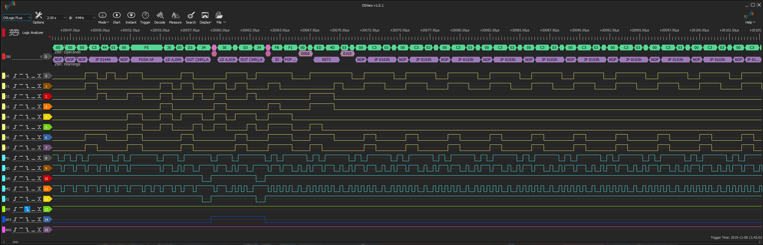
In screenshot
LA_02.png we can see the
interrupt service routine run (it starts with NOP and PUSH AF)
which sends a 0 out I/O 34h, followed by a 1. This input to pin
5 of the ATtiny85 (AR5 = ARduino pin 5) can be seen to fire as
the blue signal, second from the bottom of the screenshot. After
the Return from Interrupt instruction, RETI, the system goes
back to NOP looping.
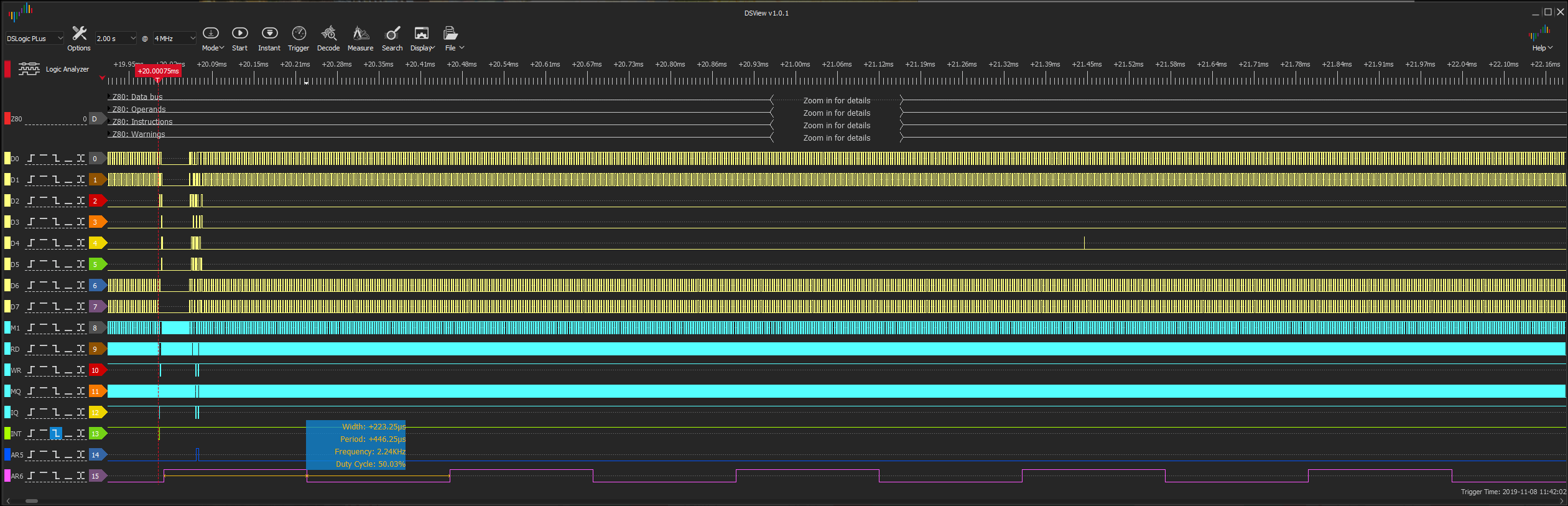
Screenshot
LA_03.png shows AR6 (ARduino
pin 6), the last (purple) signal at the bottom of the
screenshot, send out the melody/tone for the circuit to play.
LA_01.png
LA_02.png
LA_03.png
I see the schematics. Where is the Bill of Materials parts list? The BOM is at the bottom of the adjacent panel.
How big is the Serial Interface board and what will the printed circuit board look like? The PCB measures 100mm x 100mm (4"L x 4"H). Click the adjacent thumbnail to see a possible parts layout.
Note: M62 Bus is copyrighted by Peter Murray of Murray Electronics, http://www.39k.ca |

![]()
Tags: Z80 SBC, Logic Analyzer, DSLogic-Plus DSView