|
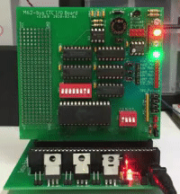
M62-bus Counter Timer Circuit (CTC) I/O Board |
| PCB Circuit (click to enlarge) | CTC Board Circuits and Info |
|
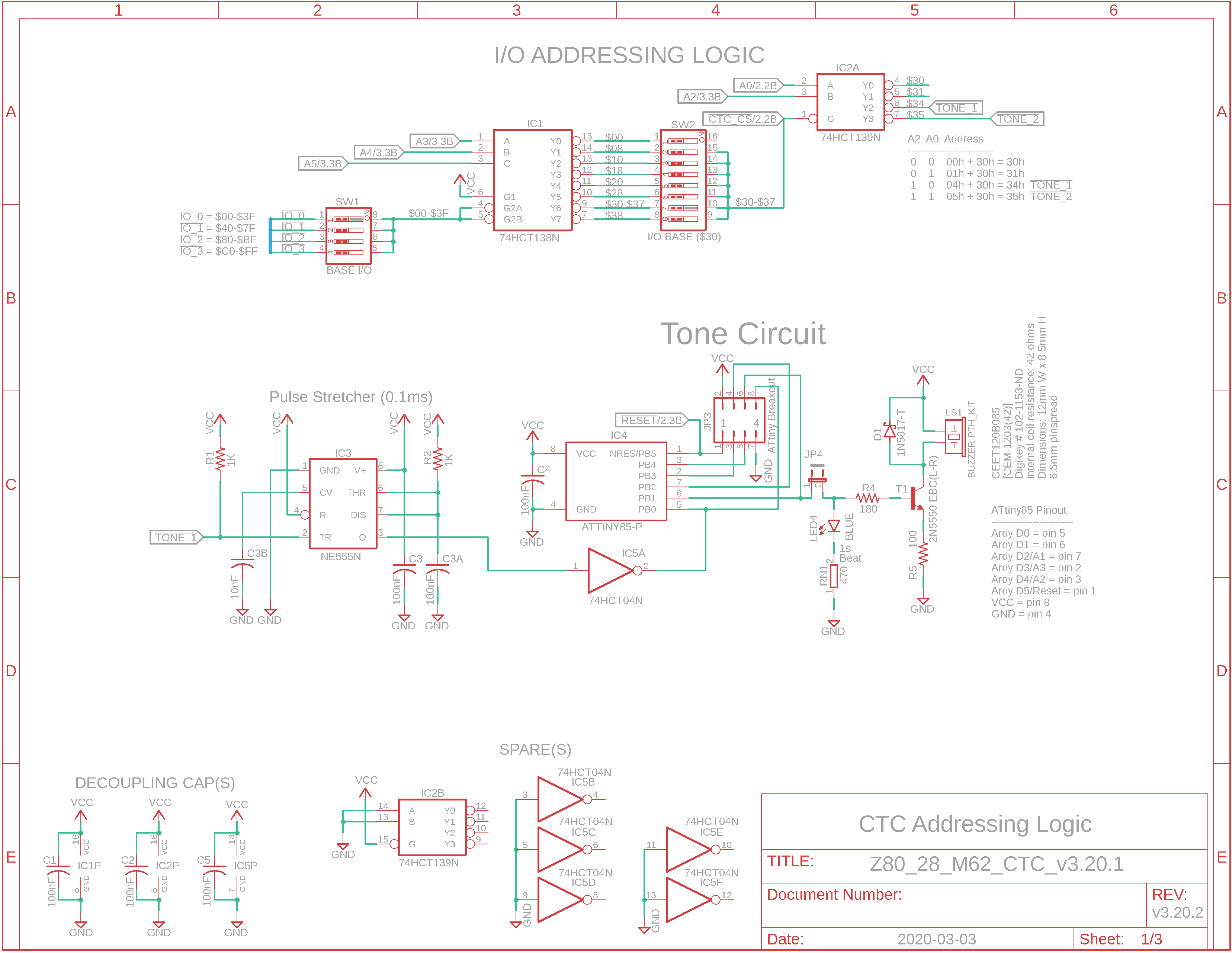
Eagle CAD: 1. Addressing Logic
Eagle CAD: 2. Counter Timer Circuit
Oscilloscope: Tone_1 Pulse (from INT) Lengthened
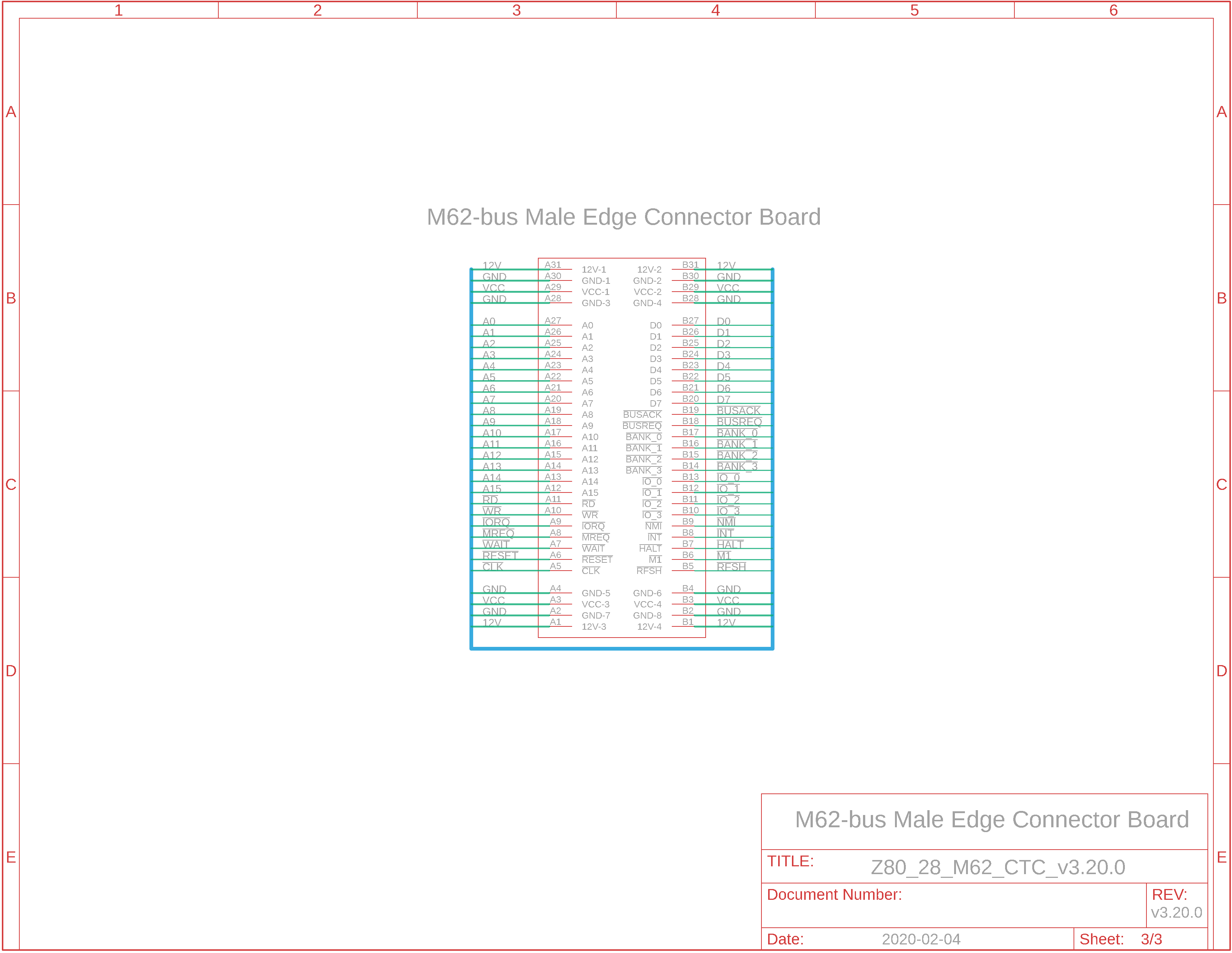
Eagle CAD: 3. M62-Bus Male Edge Connector
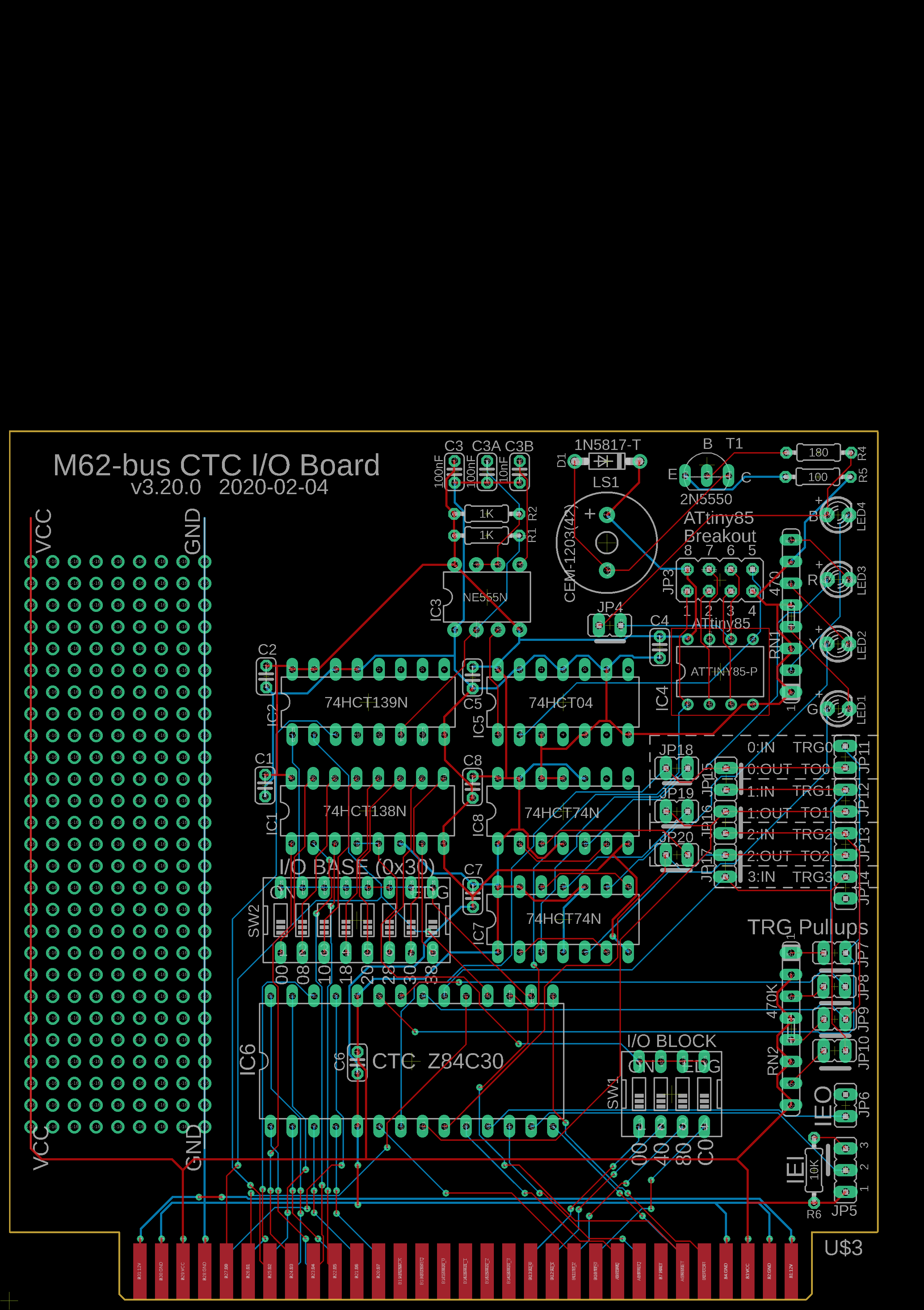
Eagle CAD: 4. A Possible PCB Layout
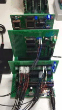
5a. v3.12.1 Video. Click for short HD .MP4
5b. v3.20.0 Video. Click for short HD .MP4
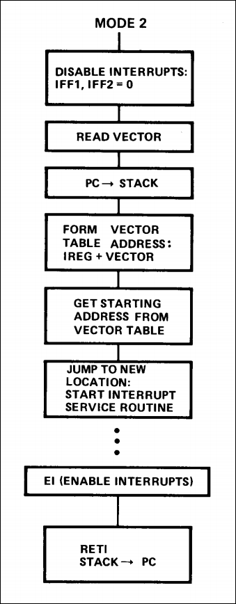
Z80 Interrupt Mode 2 (IM2) Operation
(Bill of Materials)
|
PLEASE NOTE: I do not sell production boards. If you would like to buy an M62 Z80 SBC system board/parts kit, contact Peter Murray, Peter@39k.ca I simply provide you with information to build your own breadboard computer.
Overview The M62 CTC I/O Board can be used with either the M62 SBC or SBC2. There is extensive information on the CTC, including interrupts in the Circuits section under More I/O: Z80 CTC.
Bank Addressing JP15 carves up the I/O space into for 64-byte blocks; they are: - $00 - $3F IO_0 block - $40 - $7F IO_1 " - $80 - $BF IO_2 " - $C0 - $FF IO_3 " The Z80 assembly code is written to support any I/O byte address between $00 and $3F being used. With both block and byte I/O addressing being configurable on this board, you could change it to whatever as long as your code agrees.
Block Addressing We are using the IO_0 bank of I/O addresses via the JP15 jumper between pins 1 & 2. IC1 carves that bank of 64 into 8 blocks of 8 addresses. You can use JP1 to select whichever I/O block you like; we have chosen $30 to $37 (there is a jumper between pins 13 and 14 of JP1) because it is not in use elsewhere in our Z80 system. This will become CTC_CS, the chip select for the CTC. By using A0 and A2 as inputs to IC2A, the address outputs will be $30, $31, $34 and $35. (We don't need $30 to $33 for the output TONE_1 on pin 6.) I/O address $30 to $33 will be used by the CTC chip (via the A0 and A1 pins of the CTC) so we can access the four timer/counter channels. Although we don't need pin 5, TONE_2, it's there in case you decide to do a little experimenting. (Keep in mind that it does not have pulse stretching circuitry like TONE_1 does.) The TONE_1 output goes to the ATtiny85's pin 5, PB0, that we know as Arduino pin D0. A low signal here will force a tone or melody out pin 6, PB1, a.k.a. D1.
How does it work? (Summary info is found here. The gory details can be found at Circuits section .) When an OUT instruction is sent to I/O address $30-$37, it selects the CTC so that its inputs and outputs can become active. The CTC in Timer mode uses the system CPU CLK signal on pin 15 to countdown such that a 61Hz signal is output on pin 7 which is Channel 0. The 7474's IC7A output from that input divides it by 2 so we see a rapid 30Hz beat signal from green LED1. The output of CTC pin 7 is jumpered to input pin 22 which is Channel 1. In Counter mode, the output on pin 8 is a 4Hz signal to the 7474 latch whose IC7B output is a 2Hz beat signal from yellow LED2. The output of CTC pin 8 is jumpered to input pin 21 which is Channel 2. In Counter mode, the output on pin 9 is a 2Hz signal to the 7474 latch whose IC8A output is a 1 Hz beat signal from red LED3; this is a flash every second. The output of CTC pin 9 is jumpered to input pin 20 which is Channel 3. (There is no output pin for this channel.) In Counter mode, it will count down every 1 second and send an interrupt on pin 12 to the Z80. Responding to the interrupt via its interrupt service routine, the CPU will send a low signal to address $34 which is connected to pin 5 of the ATtiny85. The microcontroller in turn will play a programmed melody/tune/chirp and light up blue LED4. More info on interrupts can be found here in the Circuits section.
What's with all the jumpers? You're probably wondering about the jumpers JP11 through JP20 in Eagle CAD: 2. Counter Timer Circuit. We know we need to jumper TO0 (out) to TRG1 (in) for the 61.035Hz signal so that's what JP15 does; you add the jumper. JP18 should be jumpered to complete the circuit to LED1. But you may want to use TRG0 and TO0 for something else instead of the LED1 circuit. In that case, remove JP15 and JP18. You can use female jumper cables to route TRG0 and TO0 at position JP11 at the board edge to the prototyping part of the board. You'll need JP16 jumpered for TO1 and TRG2 for the 1Hz LED2 circuit. JP19 completes the circuit. Removing both JP16 and JP19 will give you prototyping isolation so you can use those two signals elsewhere at JP12 at the board edge. You'll need JP17 jumpered for TO2 and TRG3 for the 0.1Hz LED3 circuit. Removing both JP17 and JP20 will give you prototyping isolation so you can use those two signals elsewhere at the board edge.
Development space: We have added some prototyping space to the left side of the board along with a couple of vertical GND and VCC lines. You can add your own devices here without having to wire to a breadboard (unless you want to).
To Do List: 1) Write the assembly code. The code for the configuration program and the interrupt service routine are cumulatively small. With the difficulty I had in getting the CTC to interrupt reliably, I ended up writing code to a) run on boot ROM (to avoid the BIOS) as well as b) standalone code to be run at $4000. 2) Program the ATtiny85 in C++ to play a tone/melody on pin 6 when it receives a low INT signal on pin 5. You'll need a programmer like this Sparkfun unit, or use an Arduino UNO as the programmer to program the ATtiny85. Here's a doc I wrote that should simplify that process: Program_an_ATtiny85.txt
Where's the software? 1) You'll need the assembly code of CTC_4ch_1int___16a.bin to run at address 4000h that will configure the CTC. Use the ROM Monitor "X" command to perform a File | Send File to address $4000. Follow this with "G 4000" to execute the file at that location. 2) The ATtiny85 won't do much unless it's programmed with the CTC_60s.ino file. 3) If you have issues with trying to get the magnetic buzzer/piezo to work properly, run the assembly program Test_IO_34h.bin at $4000 which will send a signal directly to the ATtiny85 to play the tone. 4) Initially I had some issues getting the CTC to run reliably so here's some code I wrote for a boot ROM that helped with isolating the issue: Boot_CTC_IM2__05a.bin 5) If you're just trying to test the buzzer, here's some effective boot ROM code: BOOT_CTC_IO_34h.bin
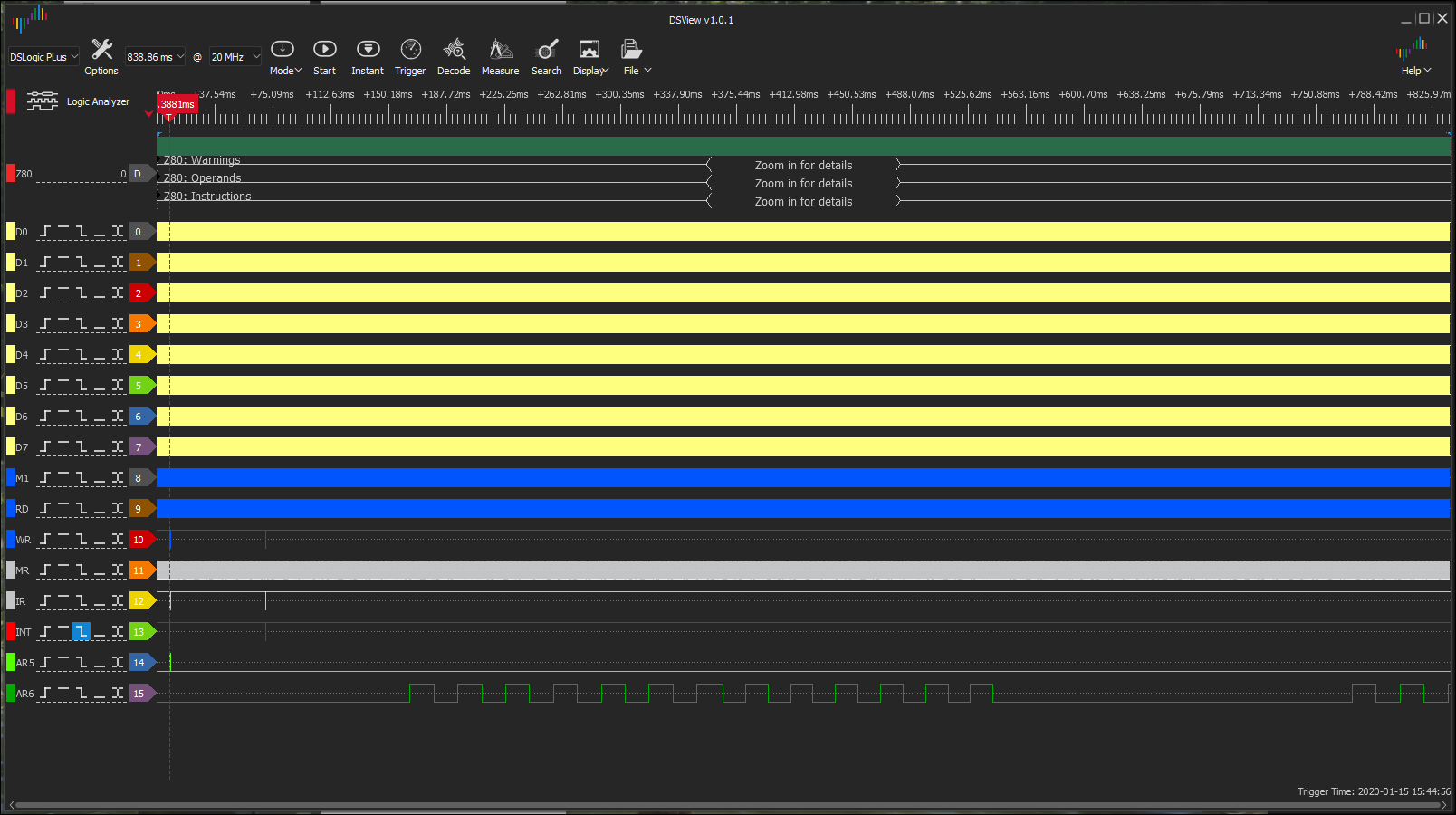
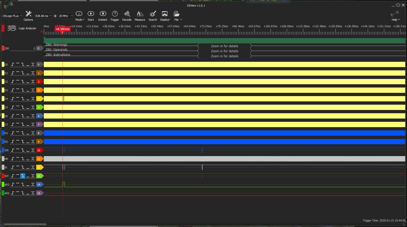
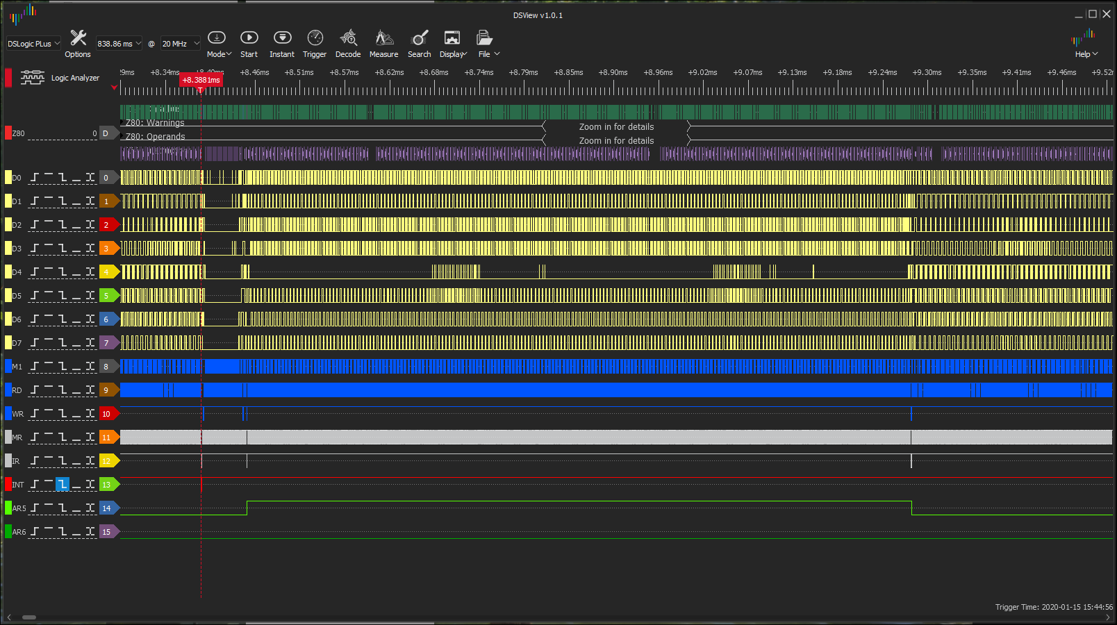
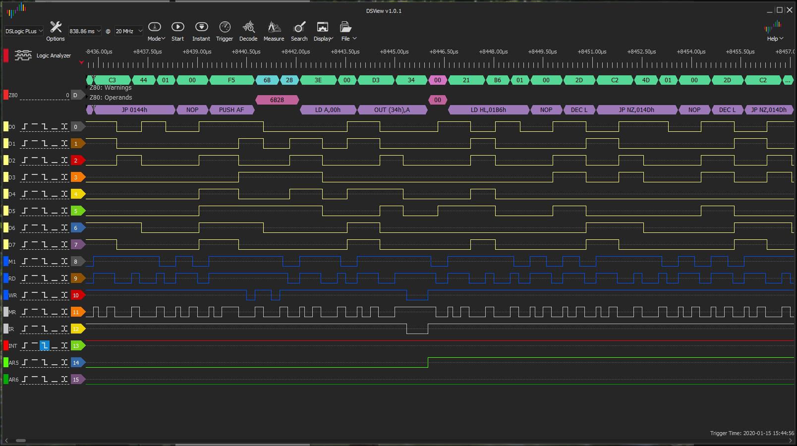
Logic Analyzer Output Below are 4 enlargeable images showing: 1) The red line on the left (third from the bottom) is the low-going trigger for INT. This causes pin 5 (AR5, second from the bottom) to the Arduino ATtiny85 to go high briefly which will trigger it to play a tone. We also see the tone being played on pin 6 (AR6, bottom) to the "piezo" speaker. 2) The display is zoomed a little to show the AR5 signal stretched a bit. 3) The display is zoomed more. The operands (green, near the top) and decodes (purple, near the top) cannot be read yet. 4) The display is zoomed enough to show the start of the interrupt routine: JP 0144h, NOP, PUSH AF, LD A 00h, OUT(34h) A, and then a short delay routine starts before LD A 01h, OUT(34h) A, EI, POP AF, and RETI. The ATtiny85 did not seem to react well to the rapid raising and lowering of D0 (AR5) so including the 1ms delay was helpful.
1)
Additional Info If you need additional info on the CTC Control Word, see page 7-60 of Osborne_4_and_8-Bit_Microprocessor_Handbook.pdf
I see the schematics. Where is the Bill of Materials parts list? The BOM is at the bottom of the adjacent panel.
How big is the CTC I/O bd. and what will the printed circuit board look like? The PCB measures 100mm x 100mm (4" x 4"). Click the adjacent thumbnail to see a possible parts layouts.
Note: M62 Bus is copyrighted by Peter Murray of Murray Electronics, http://www.39k.ca |


![]()
Tags: Z84C30, Logic Analyzer, DSLogic-Plus DSView