|
ZB64PC-bus Z80 SBC |
| PCB Circuit (click to enlarge) | Circuits and Info |
|
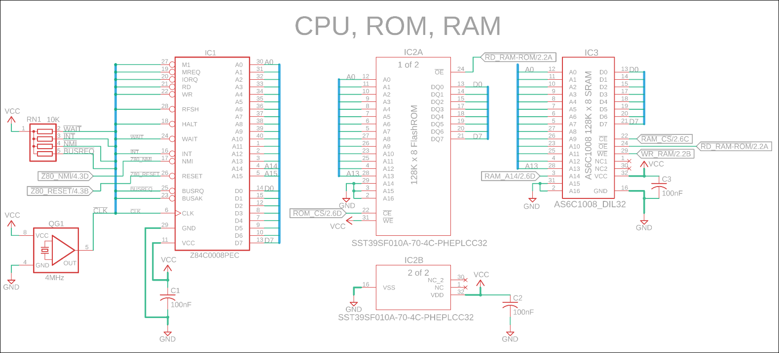
Eagle CAD: 1. CPU, ROM, RAM
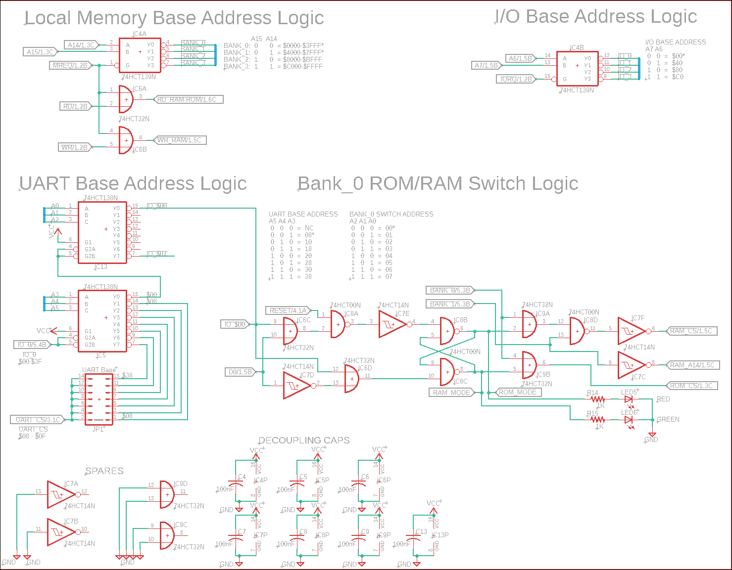
Eagle CAD: 2. Memory & UART Addressing, Bank 0 ROM/RAM Switch Logic
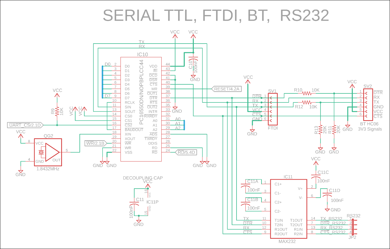
Eagle CAD: 3. Serial, FTDI, Bluetooth, RS232
Eagle CAD: 4. Function Circuitry
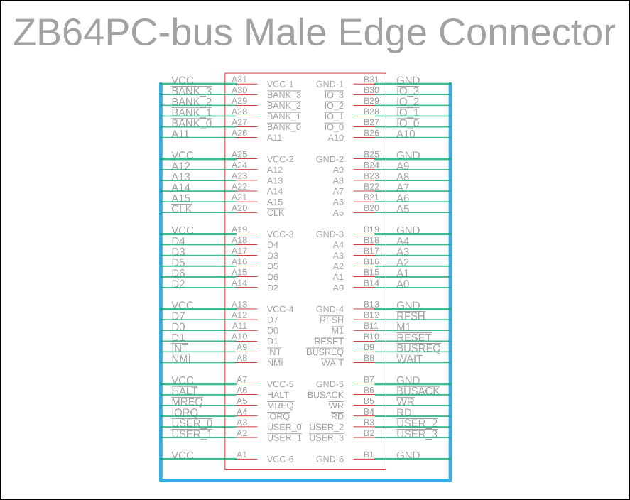
Eagle CAD: 5. ZB64PC-bus Male Edge Connector
Eagle CAD: 6. A Possible PCB Layout
(Bill of Materials) |
PLEASE NOTE: I do not sell production boards. If you would like to buy an M62 Z80 system board/parts kit, contact Peter Murray, Peter@39k.ca I simply provide you with information to build your own breadboard computer.
Overview The ZB64PC CPU boards is a single 100mm x 100mm (4" x 4") system board. Due to the through-hole density of the board components, there was barely enough room left for 5v USB power. You can use the miniUSB connector, or a multislot powered backplane and 12vDC (or higher) "wall wort" to power it.
System Expansion The ideal ZB64PC system has a ZB64PC-bus CPU board, a ZB64PC-bus 4MB Memory Expansion Board (MEB), and a 6-slot ZB64PC-bus powered backplane. This will leave you 4 open backplane slots for a VGA/PS2 Keyboard board, a Compact Flash/IDE board, a Serial Interface I/O board for SD, RTC, etc.
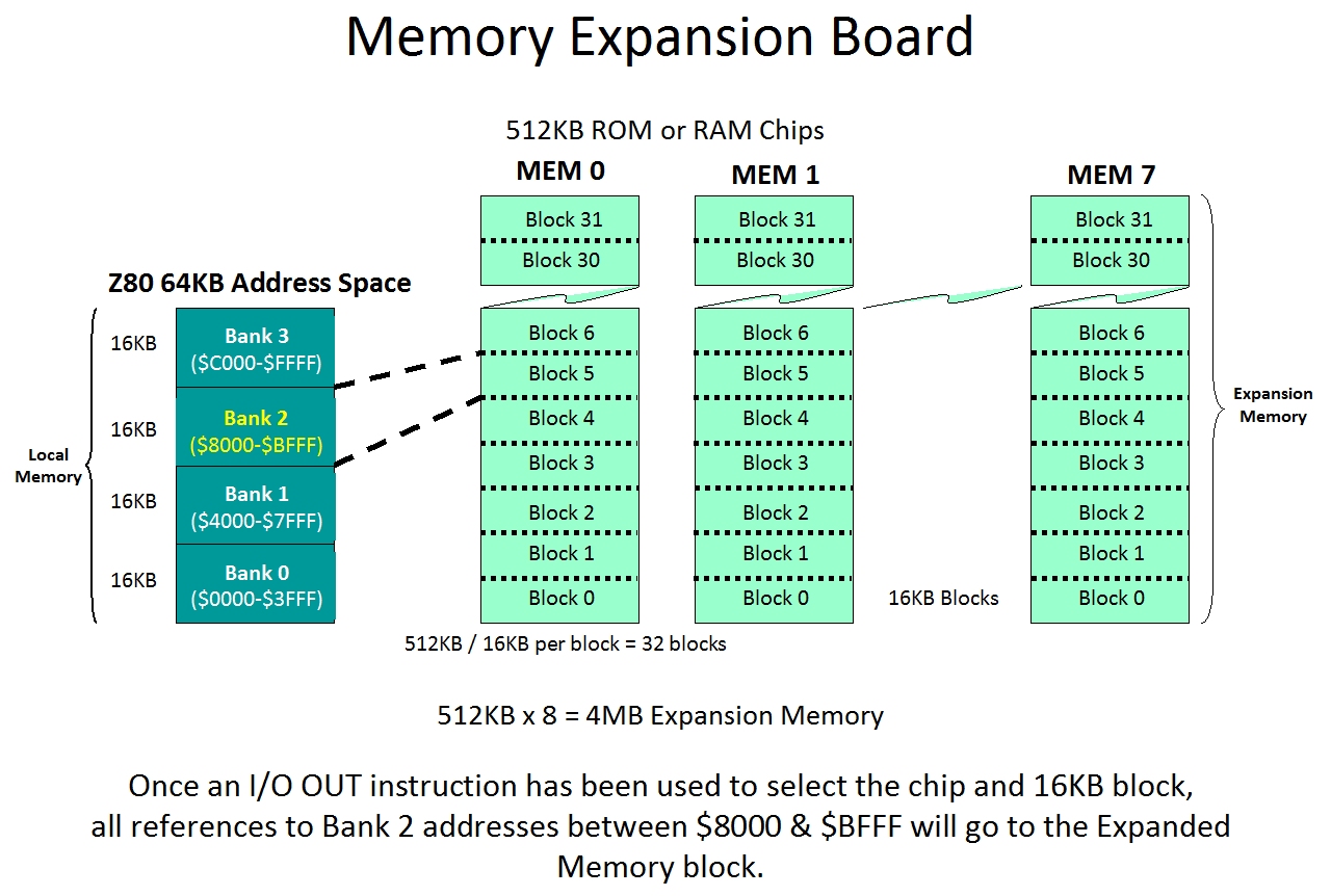
Memory Organization As you know, Z80 CPU systems are limited to 64KB of memory. The ZB64PC's 64KB memory space has been organized into four 16KB banks labeled Bank_0 to Bank_3. The four address 16KB ranges are $0000-$3FFF, $4000-$7FFF, $8000-$BFFF, and $C000-$FFFF for Bank_0 through Bank_3, respectively. Bank_0 is used by the local ROM for the BIOS, Monitor, and Operating System. This bank can be switched out for a spare 16KB block of RAM on the local 128KB SRAM chip using just a simple I/O OUT instruction. Bank_1 is used by the local RAM to run your apps. Bank_2 can be switched out by local circuitry to use up to 256 16KB memory blocks on the 4MB (4000KB) memory expansion board (MEB). Bank_3 is reserved for future development.
Organizing by Function The five adjacent schematics comprise the ZB64PC-bus design, making it easier to review its features and interconnections.
Serially Speaking The adjacent serial circuit shows the UART with its own crystal oscillator so you can choose any speed up to 115,200bps. There is a female 6-pin connector for a FTDI-to-USB module and another for the popular HC-06 Bluetooth module. There is also a female 4-pin connector in case you would like to add an RS232 connector. You should use only one of the three comm modules at a time.
How does Expanded Memory work?
Memory Bank_2 ($8000-$BFFF) is used as a 16KB window into the 4MB memory space on the MEB. By way of a simple I/O "OUT" instruction, you tell the hardware to select the 16KB Bank_2 memory block replacement from the expanded memory. You still have access to Bank_0 ($0000-$3FFF) and Bank_1 ($4000-$7FFF) locally on the ZB64PC as well as a boatload of Bank_2 16KB blocks on the MEB.
ROM/RAM Bank Switch Logic Examine the second adjacent schematic. The circuit labeled ROM/RAM Bank Switch Logic is used to switch out the ROM so it can be used for local RAM. Peter Murray has modified his M62 Operating System such that once Bank_0 ROM has been replaced by RAM in the local RAM (the SRAM chip is 128KB so there's lots of room), it copies the BIOS and vectors to the upper portion of the RAM. Now the entire 16KB (except $0000-$0100) originally occupied by the ROM in Bank_0 is available as RAM in Bank_0. By issuing an "OUT 00, 01" instruction in your programs or via the ROM Monitor menu, the RAM is expanded from $0000-$3FFF (BANK 0) to $0000-$7FFF (BANK 0 and BANK 1). This is because the BANK 0 address range which normally points to the ROM that was used to boot the Z80 now points to the first 16KB of RAM. The ROM is no longer addressed so it effectively does not exist. BANK 0 is now RAM with address range $0000-$3FFF. Now RAM exists in both BANK 1 and BANK 0. Sending instruction "OUT 00, 00" resets the configuration so BANK 0 is ROM ($0000-$3FFF) once again and BANK 1 is RAM ($4000-$7FFF). This configuration is also the default bootup configuration. Note that with the ROM excluded, you'll need to modify the boot vectors between $0000 and $0100 ($00, $38, $66) to RAM, otherwise the system will crash if an interrupt or NMI is issued because the ROM is "gone". More on that later when we talk about the M62 Operating System. Suffice it to know for now that you do not have to switch out the ROM for RAM; the Memory Expansion Board (MEB) has plenty to go around.
I see the schematics. Where is the Bill of Materials parts list? The BOM is at the bottom of the adjacent panel.
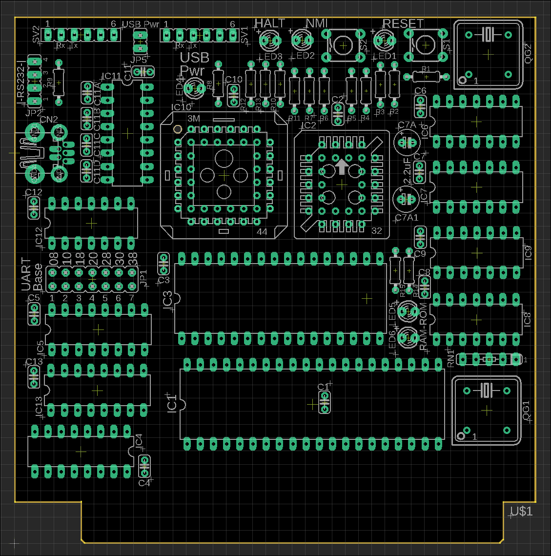
How big is the ZB64PC and what will the printed circuit board look like? The ZB64PC measures 100mm x 100mm (4" x 4"). Click on the adjacent thumbnail below to see a possible parts layout for your design.
Note: M62 Bus is copyrighted by Peter Murray of Murray Electronics, http://www.39k.ca |

![]()