|
ZB64PC-bus Memory Expansion Board (MEB) |
| PCB Circuit (click to enlarge) | Circuits and Info |
|
Eagle CAD: 1. Memory Expansion Decode Logic
Eagle CAD: 2. SRAM Bank
Eagle CAD: 3. M62-Bus Male Edge Connector
Eagle CAD: 4. A Possible PCB Layout
(Bill of Materials)
|
PLEASE NOTE: I do not sell production boards. If you would like to buy an M62 Z80 system board/parts kit, contact Peter Murray, Peter@39k.ca I simply provide you with information to build your own breadboard computer.
Overview Using your ZB64PC CPU board, you can access all of the ROM and RAM expanded memory on the MEB (Memory Expansion Board. With eight 512KB SRAMs installed, a total of 4MB is available on this board. And you can build multiple boards because each is uniquely addressed with a user selectable address jumper.
How does Expanded Memory work? In the upper left corner of ZB64PC schematic 2, we noticed there were 4 banks named BANK_0 through BANK_3 that split up the 64KB Z80 addressing system into four 16KB banks. Bank_0 was used by ROM, Bank_1 was used by RAM, and Banks_2 and 3 were available for assignment. Bank 0 swapping circuitry
(this was discussed with the
ZB64PC SBC board) could be accessed by sending an OUT
I/O instruction to I/O address $00 with value $00 for default mode,
or value $01 to change Bank 0 from ROM to RAM. That still
limited our RAM to 32KB (16KB Bank 1 and 16KB Bank 0); we may need
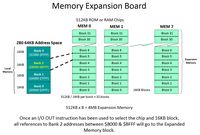
more memory. Expanded memory beyond the 64KB barrier requires we give up one bank of local memory (local to the ZB64PC-bus SBC board) so it can be used as a "window" to many 16KB banks of memory on the Memory Expansion Board (MEB). Like the ROM/RAM swapping method discussed above, an I/O OUT instruction is sent but to address $C0 that has been assigned by jumper (JP5) to the first MEB. Whenever memory attempts to use any address in Bank 2 between $8000 and $BFFF, the request will be gated to the MEB instead of to local memory. The diagram to the right shows how a local 16KB bank of memory is mapped to any of 256 16KB memory blocks for a single 8-chip Memory Expansion Board.
Analyzing the MEB Schematics MEB Schematic 1: In the lower left part of the schematic, signal IO_3 (IO_BASE 3) is used to enable the "memory expansion board number" by its jumpered address. The address currently selected with the little gray connector shown in JP5 is $C0. Unlike the 16KB memory address blocks, the I/O address blocks are limited to 256 total addresses, or four blocks of addresses. This is what we saw in ZB64PC Schematic 2: IC4B uses two address lines (A6 and A7) to give us 4 blocks of I/O addresses. A6 is the lower value of the two address lines and has a weight of $40 so each address block will be a multiple of $40: the first block is $00, the second is $40, the third is $80, and the fourth is $C0. The blocks are labelled IO_0 through IO_3. If an I/O address of $C0 or higher is used in an I/O instruction like OUT or IN, then a signal would be sent along the bus on the IO_3 line. This is how the ZB64PC CPU board communicates to the MEB via the backplane. ZB64PC Schematic 2: In the middle circuit, we see JP1 pins 1&2 jumpered so any data addressed to IO_0 ($00-$3F) would go to the UART ($08-$0F). Example: "OUT $08, 26" is used to set the baudrate of the UART. Pin 15 of IC5 could be called the Bank_Switch link and it operates the ROM/RAM swapping circuitry ($00-$01). Examples of using it would be to send "OUT $00, $01" to swap out the ROM for RAM, and "OUT $00, $00" to swap the ROM back in.
Any data addressed to IO_3 would be routed on the bus from the ZB64PC to the MEB that
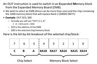
has the address $C0 selected. MEB Schematic 1: The 74573 in MEB Schematic 1 is used as an Expansion Bus Register (EBR). If you examine the circuitry beneath it, you'll see that if I/O address $C0 is used, a signal called the Memory Expansion Board Number (MEB#) is sent from the lower '138 to enable the '573 for reads or writes. The MEB# can be jumpered from $C0 to $C7 for a total of eight 4MB MEB boards using just this register. How do we select a RAM (or ROM) chip on the MEB? By sending its address to the '573 EBR. Example: "OUT $C0, 00" will output 3 binary zeroes on the 74573's pins 14, 13, and 12. This will send a zero out pin 15 of IC5, the '138 in the upper right part of the schematic. This is the CS_0 or chip select zero line.
MEB Schematic 2:
On the left side of this schematic, you can see the
CS_0
line is connected to pin 22 of the SRAM. The instruction "OUT
$C0, 00"
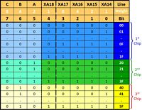
selected this chip and memory chunk. But which area of the memory will be addressed? MEB Schematic 1: When we examine the '573 EBR, we see that it uses D0 through D7 data lines. The value we "OUTed" was 00. That means pins 15 through 19 sent a zero to address lines, XA14 to XA18. These are the address lines that have been separately routed to the MEB's RAM (and ROM) but not to the ZB64PC's single ROM and RAM chips. The "OUTed" value is actually the addition of both the Chip Select line and the eXtended Address lines. The "OUTed" value of $00 points to the lower 16KB of the first chip. If the instruction was "OUT $C0, $20", that would enable CS_1 and would zero out the XA lines. XA address would be the first 16KB block at $0000. If the instruction was "OUT $C0, $21", that would enable CS_1 and would enable the XA14 line. XA address would be the second 16KB block at address $4000. Chip Select Addresses: CS_0=$00, CS_1=$20, CS_2=$40, CS_3=$60, CS_4=$80, CS_5=$A0, CS_6=$C0, and CS_7=$E0. We have selected the chip and address range but not the actual address itself: that is the job of standard memory addressing. The circuitry in the upper left quadrant in MEB Schematic 1 shows Bank 2 will be used for addressing 16KB blocks. Because the banks are organized as Bank 0 = $0000-$3FFF, Bank 1 = $4000-$7FFF, and Bank 2 = $8000-$BFFF, then the first available address in our selected 16KB block will always be $8000. If you examine the assembly code that follows, you'll see that we set $8000 as our start address. The test that follows will write $AA from $8000 to $8FFF.
Testing an SRAM chip on the MEB .org
$4000
; Location in standard memory (Bank 1) to run the assembled
application file.
Once completed, go into the ROM Monitor and read back location $8000 using Dump: every location should be $AA. Confirm the EMR contains the chip and block you specified using "IN $C0, $02". You should get the value (example $02) you put in the OUT statement because it's stored in the '244 in MEB Schematic 1.
I see the schematics. Where is the Bill of Materials parts list? The BOM is at the bottom of the adjacent panel.
How big is the MEB and what will the printed circuit board look like? The MEB PCB measures 100mm x 160mm (4" x 6"). Click on the adjacent thumbnail to see a possible parts layout.
Note: M62 Bus is copyrighted by Peter Murray of Murray Electronics, http://www.39k.ca |


