|
CIRCUIT 1-1: Z80 CPU |
| Name | Circuit Schematic (click to enlarge) | Info |
|
Z80 CPU
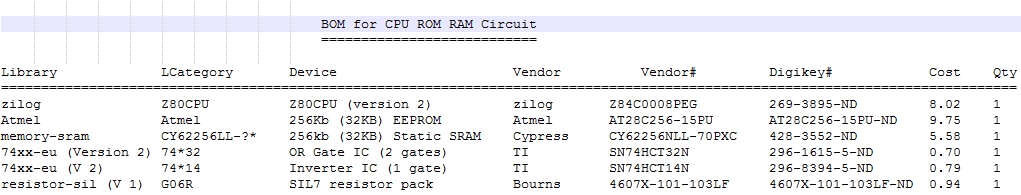
(Bill of Materials)
|
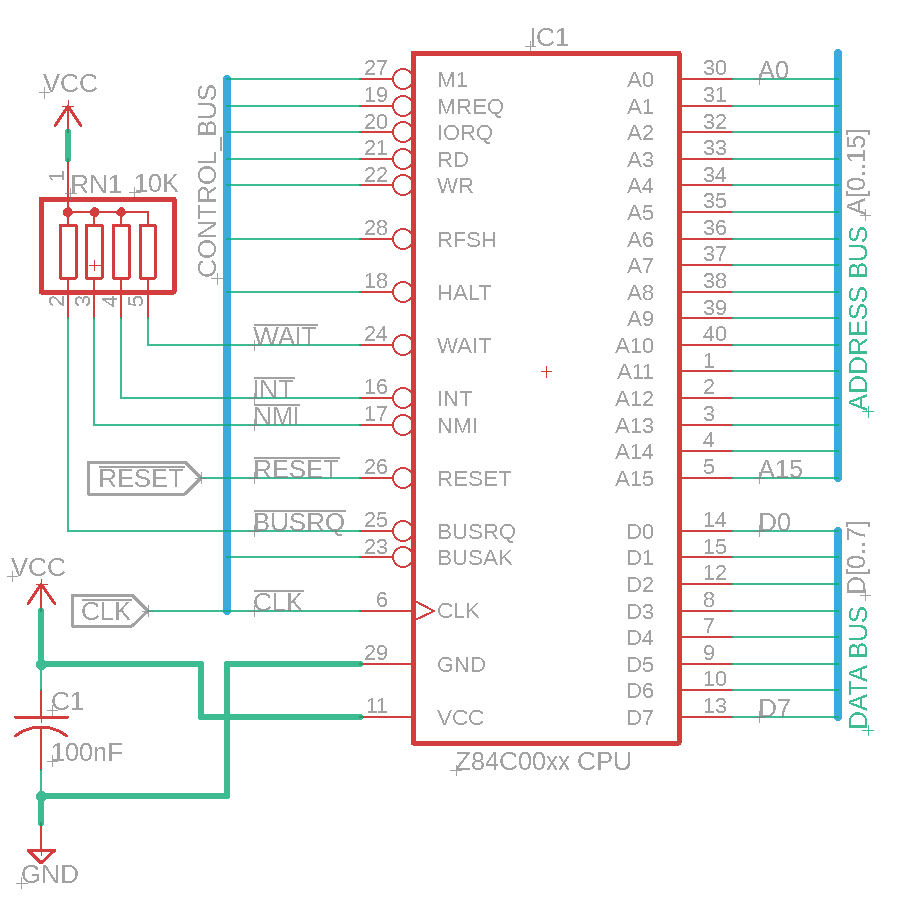
Eagle CAD: Z80 CPU Signals
|
Terminating unused CPU inputs All unused input signals to the Z80 should be terminated high: WAIT, INT, NMI, and BUSRQ. Consider using 10k resistors or a 10K resistor pack that is shown in the adjacent schematic.
Z80 RESET input signal Signal RESET will have its own circuit that is normally a logic high (1) except during use. If you're using a slow clock (the CMOS version Z84C00xx can run from DC to its silkscreened speed), you will need to manually hold RESET low for 3 full clock cycles as per the Z80 spec. The CMOS version has the letter "C" in its part number. Example: Z84C0008 The NMOS version does not have that letter. Additionally, it can only run at its labeled speed, e.g., 4MHz.
Data bus signals If you're going to run the CPU NOP Test, you really should use termination resistors to tie D0 to D7 to ground; 4.7K or a 4.7K resistor pack work well. We are not showing the resistor pack in the adjacent diagram but it's there.
Decoupling caps Don't forget the 0.1uF (100nF) decoupling capacitor that you place between VCC and the VCC power pin for the Z80. Keep it as close as possible to the CPU to attenuate the internal transistor switching spikes before they find their way into the rest of your schematic.
Test your circuit Visit CPU NOP Test to test your circuit. It contains useful info and a video demo.
Z80 Assembly Language programming Visit Z80 Programming III to learn how the Assembly code works for this circuit. |