|
CIRCUIT 1-6-1: 8255 PPI |
| Name | Circuit Schematics (click to enlarge) | Info |
|
I/O: 8255 OUTPUT with LEDs
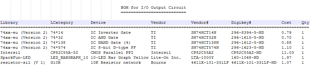
(Bill of Materials)
|
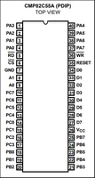
Eagle CAD: 82C55A PPI and Display Logic
82C55A Pinout
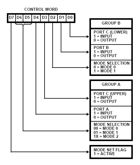
8255 Configuration Mode Definition Format
for the Control Word
Register
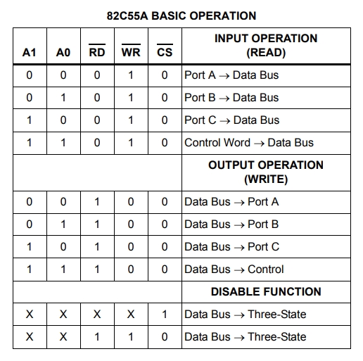
8255 Basic Operation
|
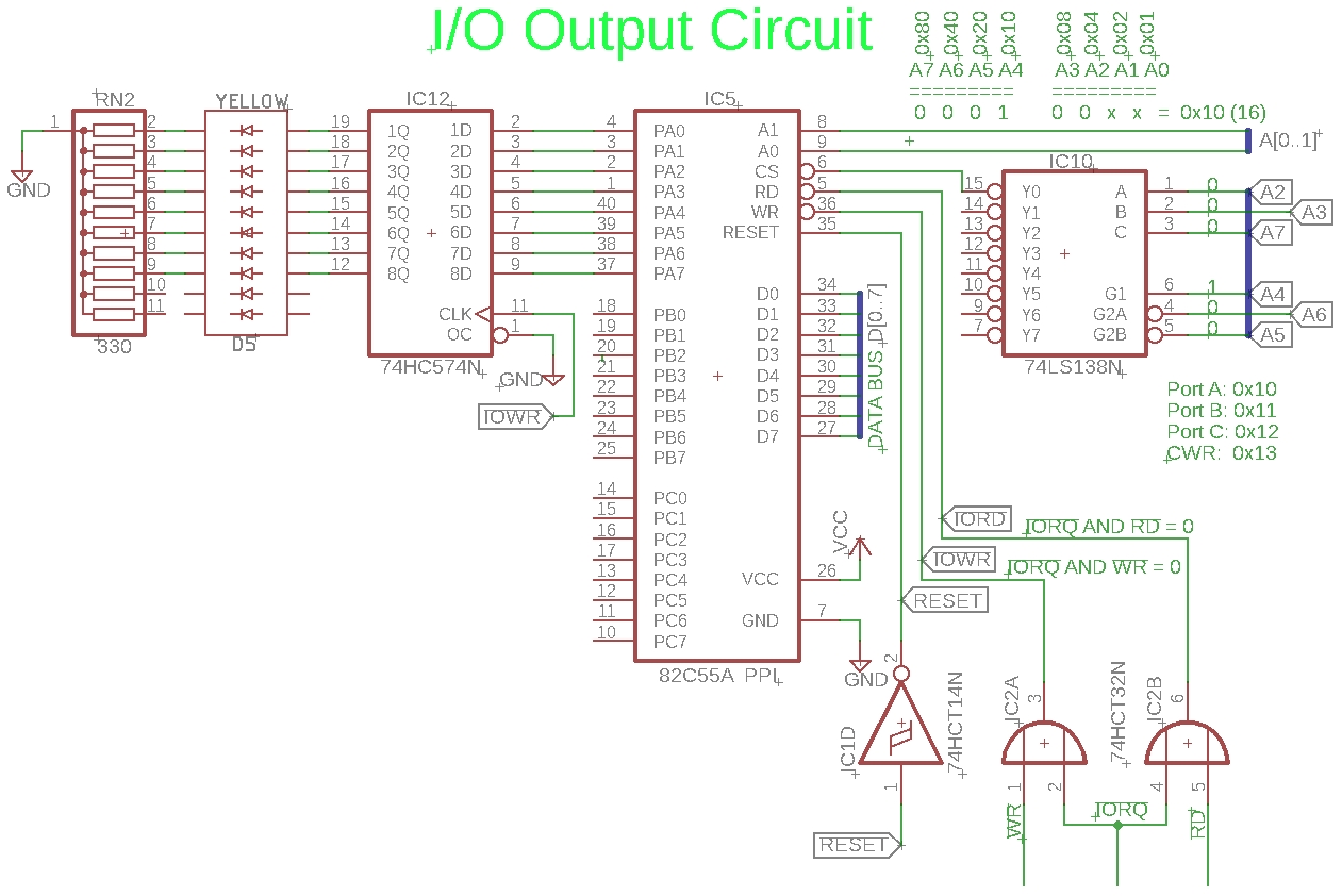
This circuit, via more addressing glue logic, will connect an 82C55A Programmable Peripheral Interface (PPI) to our Z80 CPU. We will focus on the output aspect of this input/output (I/O) device. The output will drive bar graph LEDs.
The Z80 IN() and OUT() instructions use IORQ & RD or IORQ & WR, D0-D7, and A0 to A7. Generally speaking, they do not use the upper 8 bits of the Address Bus so there are only 256 possible I/O addresses.
In the adjacent schematic, address line A4 connected to the 74HCT138 is the only line asserted positive. With A2, A3, and A7 low, output line Y0 will be selected if A5 and A6 are also low. Using A4 as a positive input to G1 to enable the '138 lets us select 0x10 as the starting address. If instead we chose A3 for G1 input, then the first address would be 0x08 up to 0x0B. If instead again, we chose A5 for G1 input, the first address would be 32 or 0x20; A6 would be 0x40; A7 would be 0x80. Looking at the binary weight table above the 74HCT138 3-line to 8-line Decoder in the adjacent schematic, we can see that usable addresses will begin with 0x10 (16 decimal).
The 8255 PPI (programmable peripheral interface) has only 4 user registers, hence the reason only A0 and A1 from the Address Bus are used. The '138 selected base address is added to the value chosen with A1 and A1: - Address binary 00 (address 0x10) is for Port A input/output (I/O) - Address binary 01 (address 0x11) is for Port B I/O - Address binary 10 (address 0x12) is for Port C I/O - Address binary 11 (address 0x13) is for the Control Word Register (CWR)
The ports are grouped into the following control blocks: - Group A: Port A, Port C upper (C4-C7) - Group B: Port B, Port C lower (C0-C3) We will be using Group A at a later date when we build a printed circuit board for the 20x4 LCD.
The CWR control word is shown adjacent. By setting the 8-bit byte to binary 1000 0000 (hex 0x80), we'll activate the 8255 and set all 3 ports as outputs in Mode 0 (basic input/output). The two other modes are Mode 1 Strobed Input/Output and Mode 2 Bidirectional Bus.
We are using only Port A of the 8255 PPI. Once the 8255 device is addressed with 0x13 to set the control word (CWR) of 0x80, we can send data on the Data Bus to address 0x10 for Port A.
The 74HCT574 is a latch that uses the IOWR signal (from the mating of WR and IORQ) to clock the data to the LED bar graph.
Test Your Circuit Visit Input/Output Test I to test your circuit. It contains useful info and a video demo. |
![]()