|
Z80 Programming V |
|
UART Serial Interface |
|
Overview: So far we have looked at the assembly code for the NOPs circuit that tested the ROM, as well as the block fill code that tested the RAM. Now we'll look at the code needed to drive a serial interface circuit. This will allow us to use our PC running terminal emulation software like Tera Term to access our Z80 system. The PC will effectively provide the keyboard input and display output. At a later date, we'll build a console such that we won't need the PC - our Z80 will have its own LCD display and PS2 keyboard, but that will be sometime later.
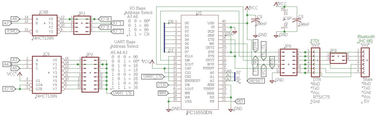
Breaking out the hardware: The schematic below looks a little busy, so let's break it down into its essential components. Starting from the upper left, the '139 allows us to break up the I/O into four regions: those identified as IO_0 with addresses $00 to $3F, IO_1 with addresses $40 to $7F, etc. There is a little table labelled I/O Base Address Select to the right of the '139 circuit that shows the I/O address blocks. The '138 below the '139 allows us to choose which address grouping we'll assign to the UART, 16550.
When an IORQ signal is
sent as the result of an OUT or IN instruction, the '139 is enabled on
pin 15 and outputs the address as received on A6 and A7. With two
inputs, A6 and A7, there are 4 possible outputs as can be seen in the
table adjacent to that circuit. On JP3, you can see we have jumpered
pins 1 and 2 for IO_0
meaning that any address sent that is lower than 64 ($40) will enable
IO_0.
IO_0 is connected
to pins 4 and 5 of the '138 below the '139. The '138 is an address
selection tool as well. We know if A3, A4, and A5 are low, then the
address will be below $08 because the value of A3 is 8. We would like to
use 8 to address the UART; We put a jumper on JP2 between pins 3 and 4
so address $08 will output the
UART_CS signal to the UART. You can see
UART_CS as the output of
JP2 and the input to U1 (the 16550 UART) on pin 14. Long story short: if the
I/O address is below $40 and equal to $08, then the UART will be
chip-selected. Could we use this same '138 to select other devices? The
answer is Yes, providing the other JP2 connections are unique to your
desired chip select(s).
Ok, now that the addressing is out of the way, we can move our eyes to the right of the addressing section. U1 is the UART, the universal asynchronous receiver transmitter. It will take our bytes, turn then into bits and them send them sequentially out any attached interfaces, probably to our PC running terminal emulation software; the PC will display them in a terminal window. Is there any guarantee that the letter "X" you typed will be received as an "X"? Nope. Does the terminal know when you're going to type "X"? Again, no because the communication is asynchronous with time. So, a START bit is added to the 8 bits of data as well as a STOP bit to frame the data. A PARITY bit can also be added so we'll know if something changed. Want more info on serial framing protocols? Try here and navigate to Rules of Serial. Ok, so the UART has quite a bit of work to do. It also has to adopt a role - DTE or DCE. DTEs are traditionally referred to as terminals and DCEs as modems. The signal is digital between DTE and DCE and is limited to only a few feet in distance. At the DCE component, it is converted to analog where it can travel much further but not as fast without a lot of special gear. Anyway... that's what all the control signals on the right side of the UART are all about. Generally speaking, we could tie them all low and the system would communicate fine but some terminals are picky and want to see either DTR or RTS from your DTE-type UART, or they want to see DSR or CTS from your DCE-type UART or they won't work. So we provided DTR/DSR and RTS/CTS in the usual FTDI pin locations to keep them happy. You'll notice we did not include the MAX232A, DB9 connector, and RS232 circuitry in this schematic: it's less busy that way. Some of you may have noticed there are two single inline female connectors for both serial-over-FTDI and serial-over-Bluetooth adaptors. You'll need to jumper TxD and RxD between the connectors to use Bluetooth. A word to the wise would be to disconnect the USB cable from the FTDI adaptor if you're going to run Bluetooth, otherwise things get weird. Either adaptor board will communicate serially over your USB cable or Bluetooth to your terminal software. You'll need to configure Tera Term for the right COM port for your adaptor. NOTE: The USB/FTDI board gets its power from the 500mA USB connector. If you have turned power off to your PCB or breadboard, the FTDI board will try to power it through its VCC line and also through the TxD line. Eventually the board will "cook" and stop working. Actually, when you reset the BIOS, you'll see it on your PC screen but won't be able to communicate through the USB/FTDI board to your Z80 because the TxD line is cooked. Consider putting 2K2 (2.2K ohm) resistors in line with all 4 comm/control lines as I have done on my ZB74-bus design. |