|
Input/Output Test IV |
| Input (4x4 Keypad) and Output (LCD Panel) using an 8255 PPI | Resources |
|
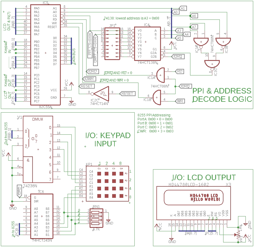
Overview: - In this test, we're going to use a 4x4 keypad to send alphanumeric characters 0-9 and A-F to a 2x16 Character LCD module - The 8255 port configuration is as follows: Port A: send either a command (clear screen, etc.) or data (0-F) to be displayed on LCD Port C high nibble: assert 3 LCD control lines Port B: sequence output to 4 keypad column lines Port C low nibble: sequence input from 4 keypad row lines to detect any key press
How does the circuit work? - There are there are 3 control pins RS, R/W and E on the LCD in addition to the 8 data pins. One of the data pins, D7, can be used by the 8255 to poll the LCD panel to see if it's busy; we won't use that function. - R/W is set to Write mode (0) as data is always sent from the microcontroller (MCU) to the LCD module and not in the opposite direction. - RS is the register select pin. This pin allows the LCD module to decide if data coming from the MCU must be interpreted as an LCD command, or if it must be treated as text data to be displayed on the LCD screen. - E enables LCD access for each MCU-to-LCD transaction. As soon as a communication starts from the microcontroller side, this pin must be put high to enable the LCD. On some LCD display controllers, you need to pulse this line low after pulsing it high. On others, it returns to low level once the procedure is completed.
How do we let the user know which key was pressed? - As we learned in Input/Output Test II utilizing the 4x4 Keypad, four distinct binary patterns are sequentially sent on PB[0..1] to sequentially output a high signal on the '238 demux to the 4 keypad columns which are tied low via termination resistors. When a key press is made, the circuit is completed and we see a high on input PC[0..3]. The vector of the column and row tells us which key was pressed. In this code, the assembly program sends the ASCII value for the 0-F key press to the LCD for display.
Examine the assembly code below for I/O Output Test III: - Assembly file, Keypad-LCD-09_PPI-Address-00h_4, is heavily documented in the first 93 lines. The document defines how the two devices are configured and used with the 8255 PPI. Lines 72 to 78 show the keypad keys matrix.
In summary, the code executes as follows: - Configure the 8255 ports as per the schematic such that only PC[0..3] are inputs, and all others are outputs - Write 38h as an initialization command to the LCD - Write 4 other configuration commands to the LCD to clear the display, set the starting DD RAM address, hide the cursor, and set entry mode 6 - Sending commands or data (eventually) to the LCD via the 8255 requires first asserting 2 LCD control lines attached to PC[4..7], then pulsing a third LCD control line, the Enable line, high then low to latch in the line state and command/data - Once this code is complete, each of the 4 keypad column lines are asserted high sequentially while we read the 4 keypad row lines looking for a key press - A key press is the vector of a particular column and row. The display routine will send a unique ASCII code for each of the 16 different key presses to the LCD for display - Because any key can easily be held down long enough to produce multiple sequential displays of the same key, a configuration command is sent to the LCD after each key press forcing it to "home" the cursor hopefully stopping the potential duplicates from being displayed - The program loops forever waiting for the next key press
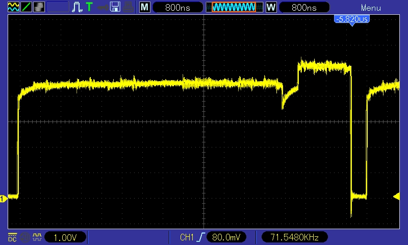
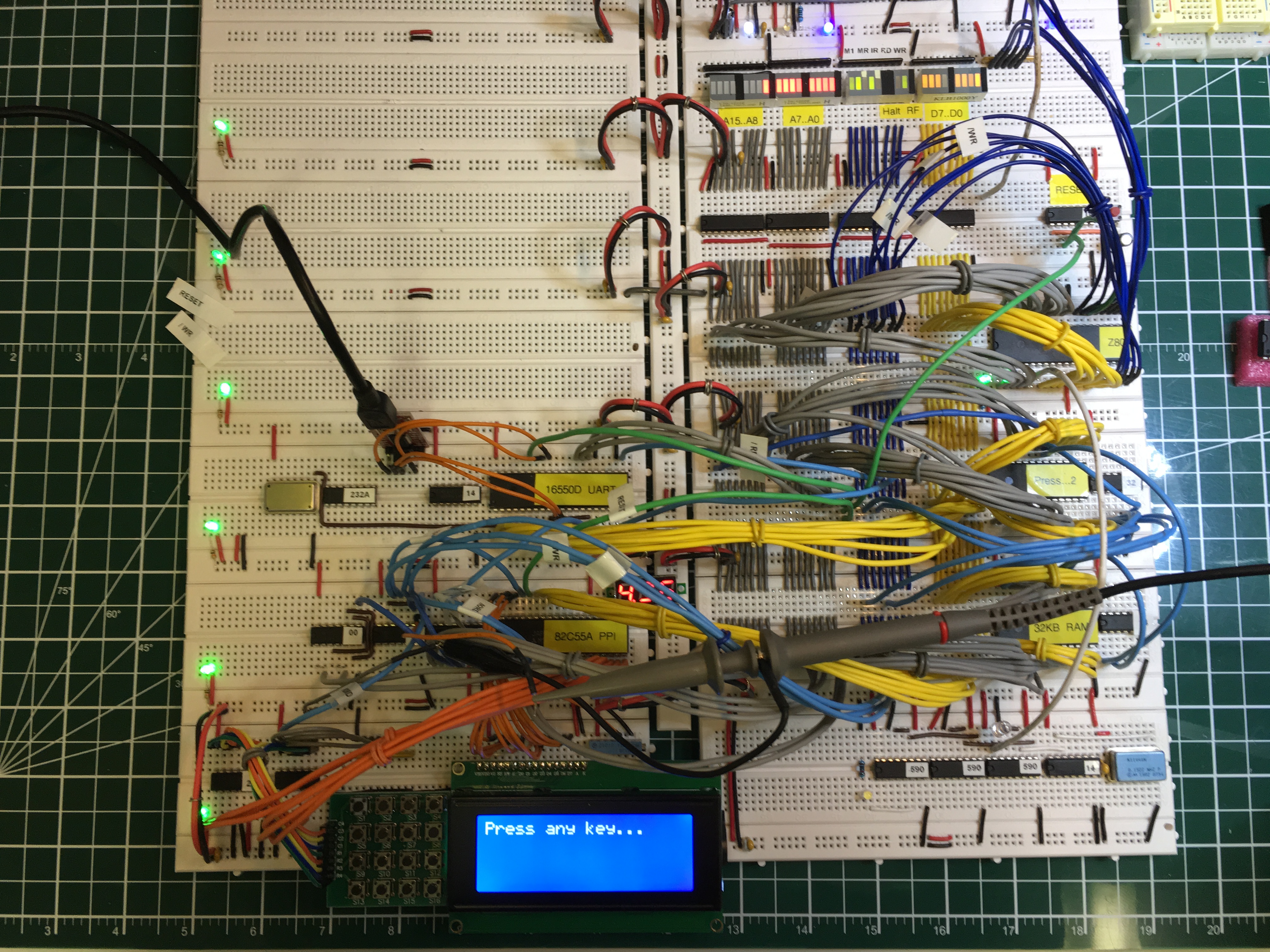
Troubleshooting this circuit: - I could not get the LCD to reliably display the text string, nor could I get it to not duplicate any key press. It made sense to work on the string issue first. In the adjacent screenshot, Troubleshooting I, you can see the LCD data is scrambled, sort of - After examining everything related to the 8255 and its peripherals, I started scoping out the actual signals. Beside the first screenshot is another showing what the scope read from the 7432 OR gate: the signal had a weird dip/bump in it. I pulled out the chip and noticed it was a 74LS32, not a 74HCT32. It seems this was what I had used while I was waiting on my Digikey order for the other HCT chips to arrive - Swapping out the LS for an HCT resulted in the 2 screenshots shown under Troubleshooting II to the right: the LCD reads "Press any key..." as it should, and the signal appears less "bumpy". Yes, there's still noise on the 5v level, but this is a breadboard build after all... - If you can't get anything to display on your LCD, look for the 8255_CS signal with your scope. It should look like the adjacent signal under Troubleshooting III. If it does not exist, work backwards from that signal source to determine what is not producing it
How do I get this program onto my EEPROM? - The Keypad-LCD-09_PPI-Address-00h_4.zip file contains the .asm file, a .lst file showing the machine code and assembly language, an .obj file that contains just the machine code, and a .hex file. The hex file is in Intel format which is used by most "burners". - Up until now we have been limping along using a file I built for you so you could load it into your Arduino-based EEPROM burner. The files are now getting much bigger and taking too long to build. It's time to consider buying a real EEPROM burner. Here's one that I have been using since June 7, 2018. It's easy to configure, easy to setup, easy to use each time, and is very reliable: it's a TL866 II Plus. Don't get the plain TL866 if you can afford the TL866 II Plus. I bought mine on eBay for $54.14us with free shipping, and it took 2 weeks to arrive from Shanghai CN
|
Input/Output Schematic
LCD Instructions
Video: Keypad - LCD Test
Clicking the thumbnail gif above will provide an HD video (4.1MB, .mp4 format)
Troubleshooting I:
Troubleshooting II:
Troubleshooting III:
|
|
20 x 4 LCDs - If you have one of these 20 columns by 4 row LCD panels (parallel only, no serial comm like I2C, SPI, etc.), you can use the Keypad-LCD-09_PPI-Address-00h_5.zip file to test it - This program
displays any key pressed on a 4x4 keypad onto a 2x16 LCD panel.
Initially the display reads "Press any key...". Afterwards, the
display is "homed" to the second row and any key press will show in
the display - The Z80 was clocked at 4.09611 MHz for a no-name HD44780-compatible 4x20 8-bit parallel LCD display |
Video: 20x4 Keypad - LCD Test
Clicking the thumbnail gif above will provide an HD video (8.4MB, .mp4 format)
DDRAM Address for 20 x 4 LCD Display
|


