|
M62-bus 64KB Z80 SBC v2.0 |
| PCB Circuits (click to enlarge) | Circuits and Info |
|
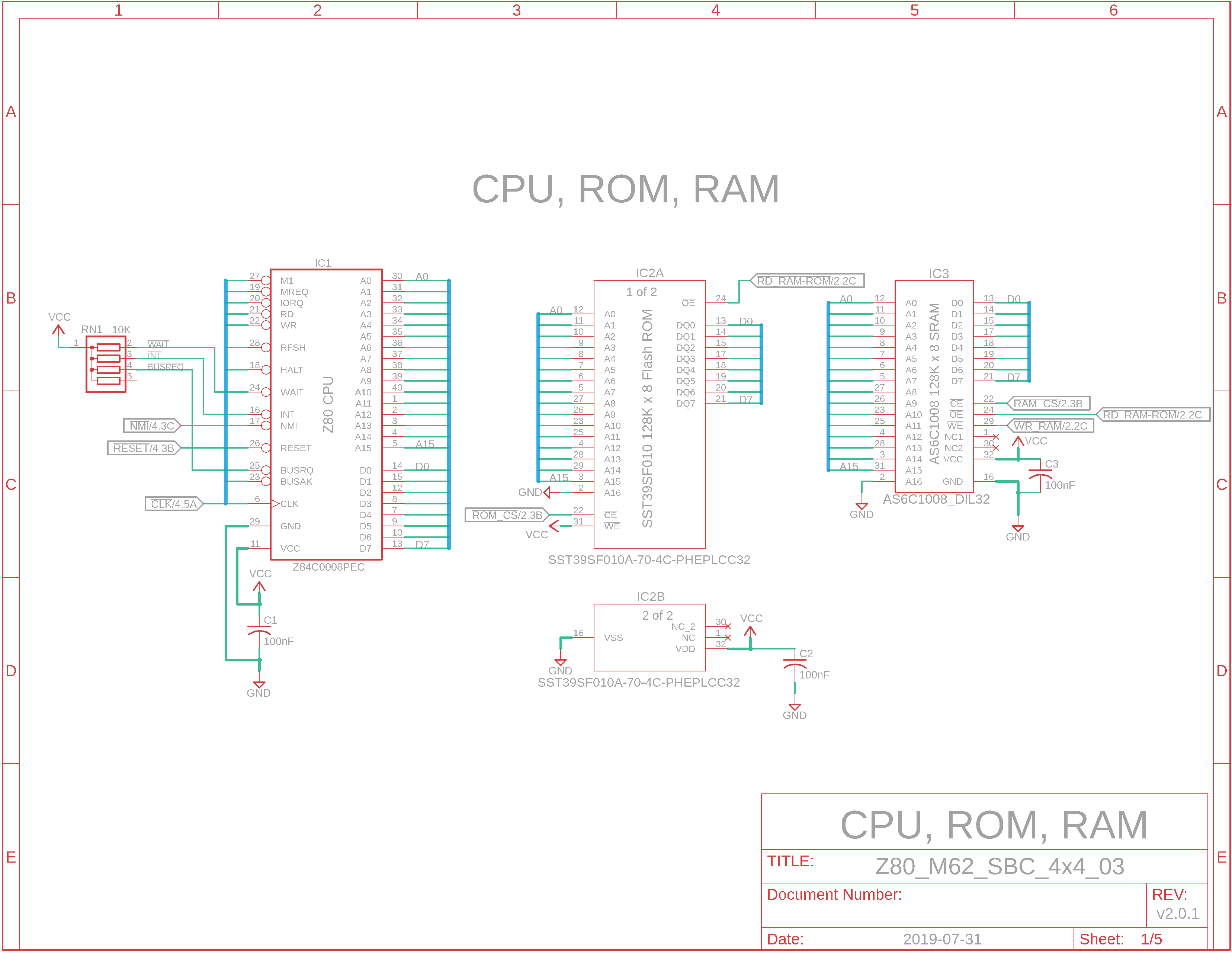
Eagle CAD: 1. CPU, ROM, RAM
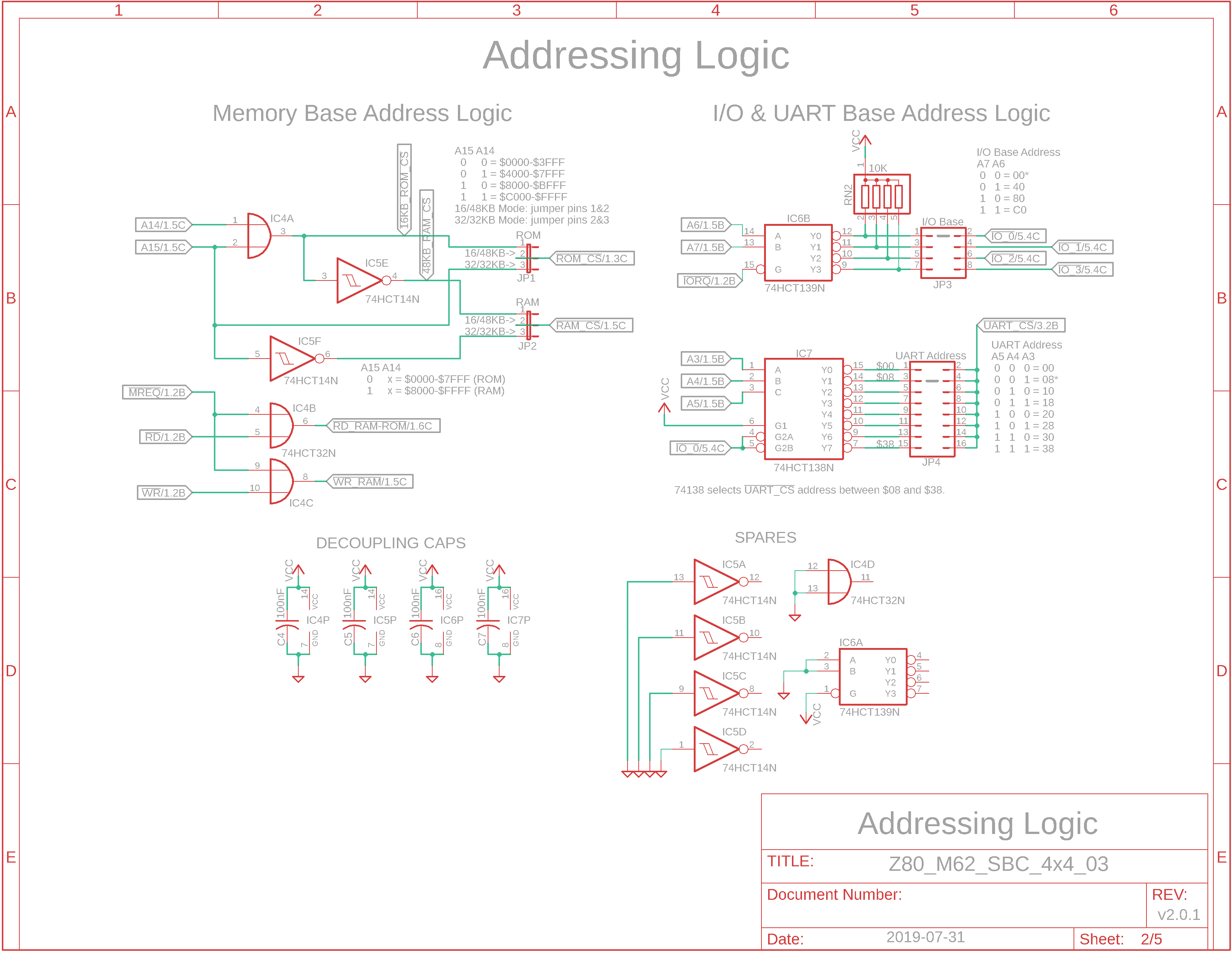
Eagle CAD: 2. Memory & UART Address Decode
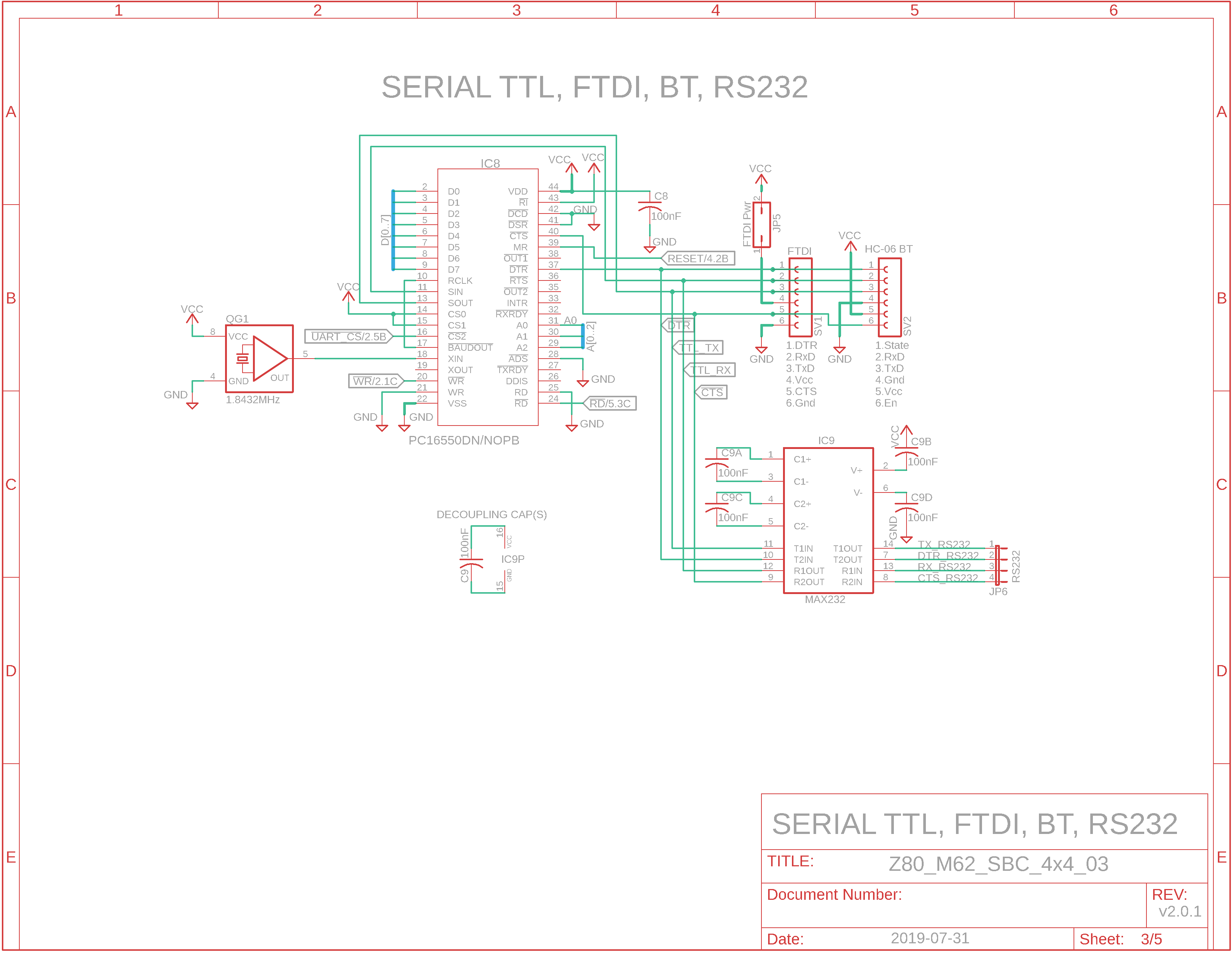
Eagle CAD: 3. UART, Serial FTDI, BT, RS232
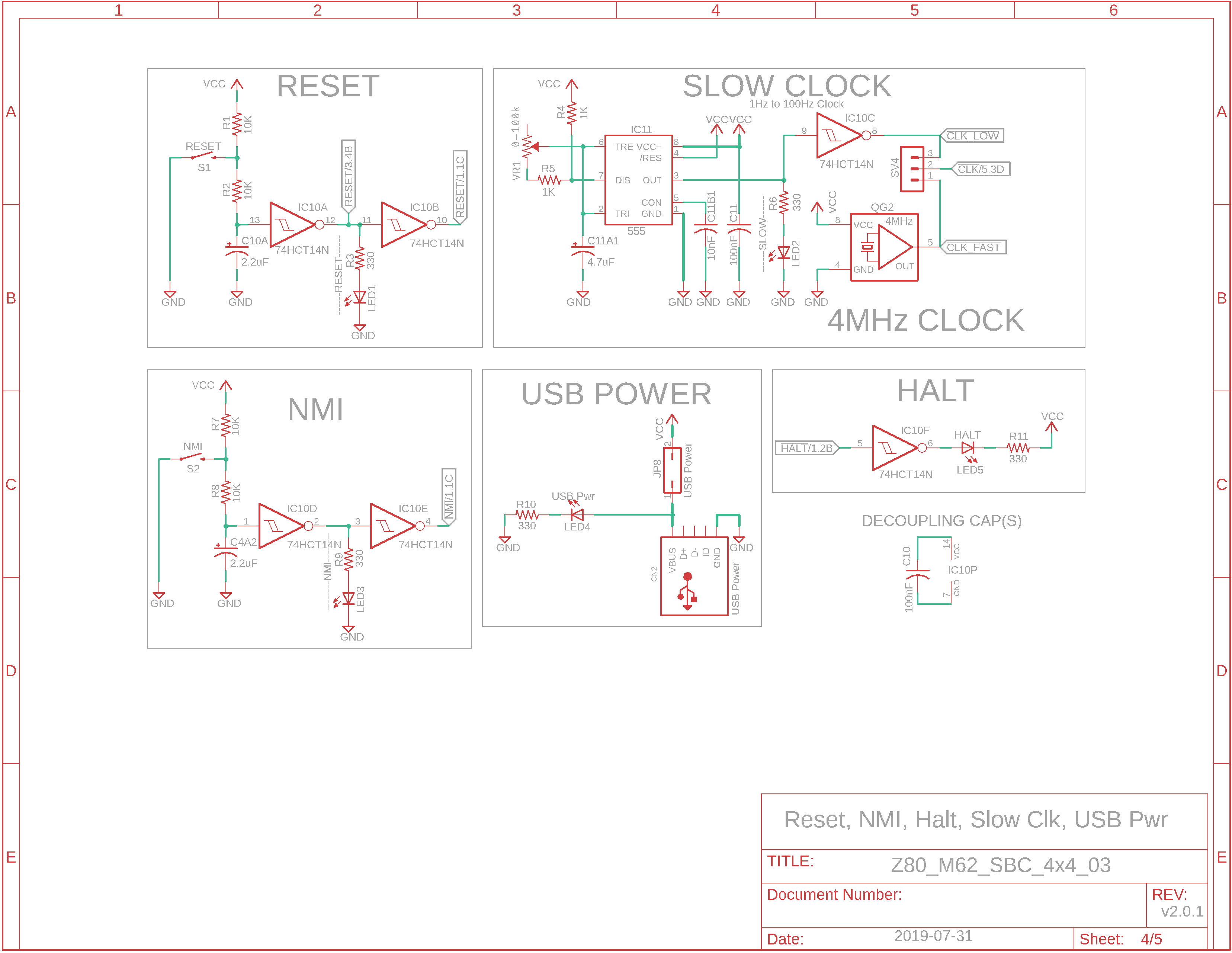
Eagle CAD: 4. Clock, Power, Reset
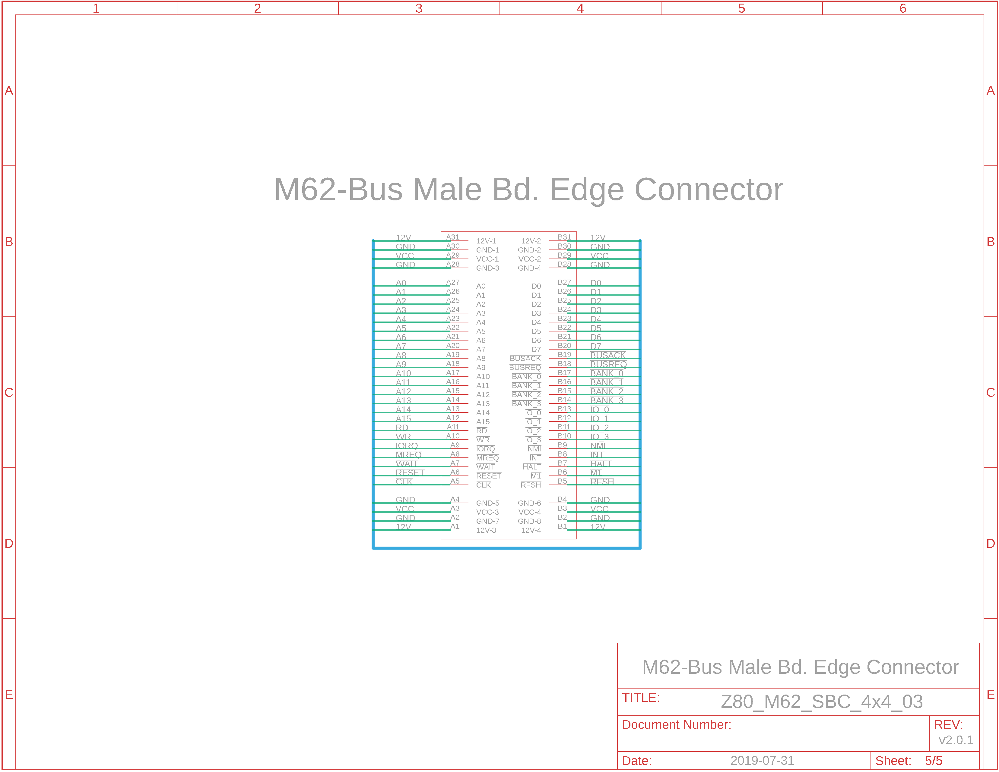
Eagle CAD: 5. M62-bus Male Edge Bd. Connector
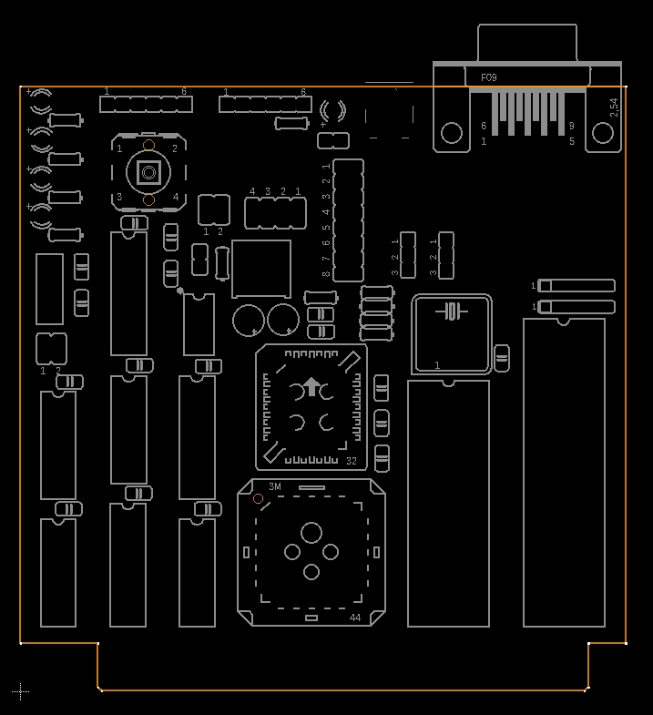
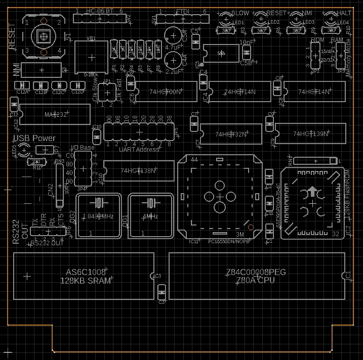
Eagle CAD: 6. Three Possible PCB Layouts
(Bill of Materials)
|
PLEASE NOTE: I do not sell production boards. If you would like to buy an M62 Z80 system board/parts kit, contact Peter Murray, Peter@39k.ca I simply provide you with information to build your own breadboard computer.
We're going to call your single board computer design, the SBC. Aptly named, don't you think?
I have built three different versions of the Single Board Computer. The one I prefer the most does not have an RS232 9-pin connector but it does have a 4-wire socket if you wish to wire a 9-pin D-sub connector to the back panel of your Z80 project. The connector was removed because most people will communicate with their Z80 using their PC's USB cable to the FTDI module or via the HC-06 Bluetooth module. Not everyone wants to assemble a powered backplane to plug the SBC into so I've included a miniUSB connector on the lower left side of the board; it's strictly for 5v power. Using just one oscillator as both your CPU clock and UART clock greatly reduces your communication speed choices so I designed the board to have both a 4MHz one for the CPU and a 1.8432MHz oscillator for the UART. Now if you want to bump up your baudrate from 9600 to 115,200bps, you can.
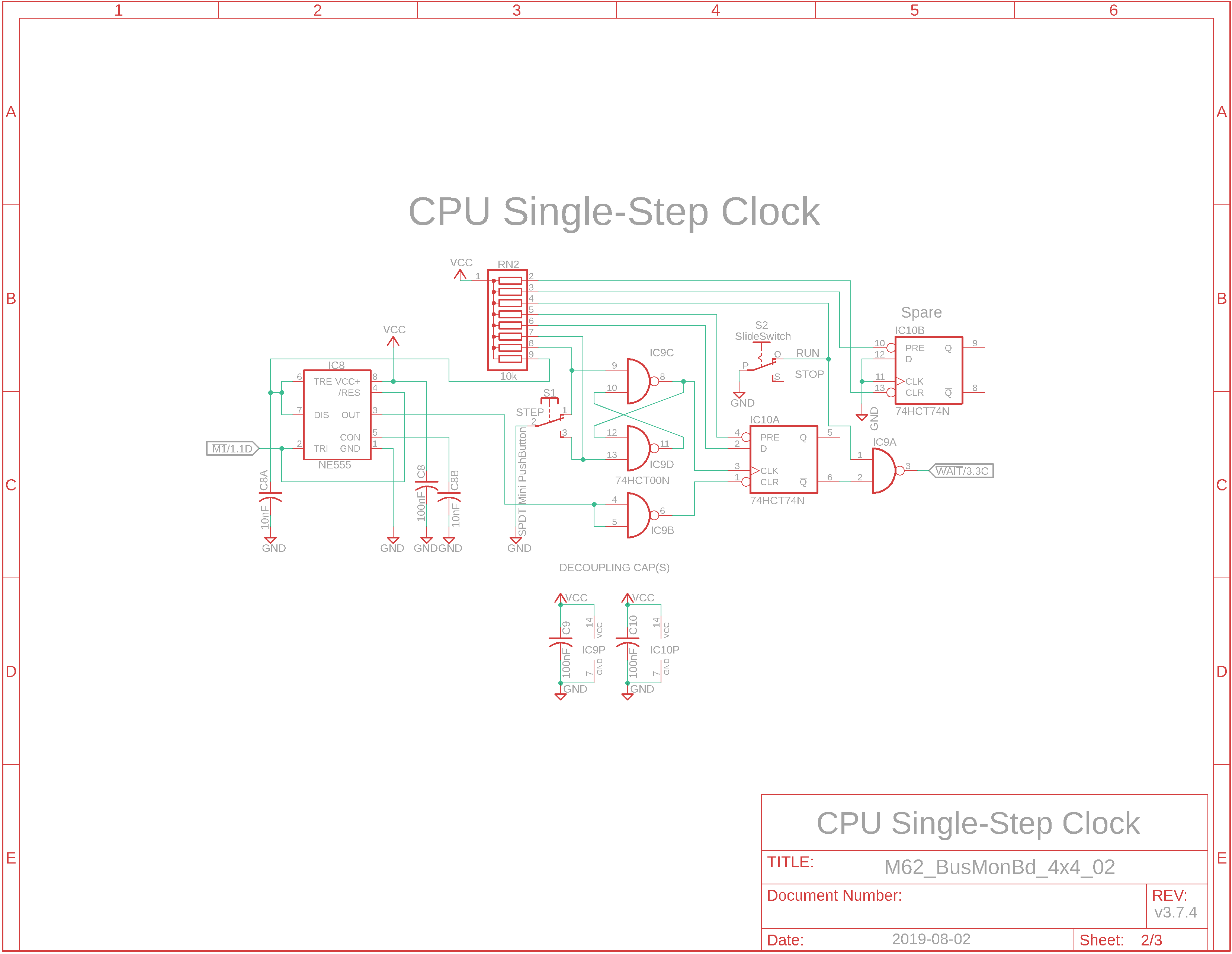
Noteworthy: 1) If you build the Bus Monitor board you could consider using the Slow/Fast Clock circuit to switch between fast (4MHz) and slow (1 Hz to 100Hz) in addition to the single-step circuitry. The latter single-steps the CPU using the WAIT (active Low) input signal to the Z80. The Bus Monitor board will show you the address and the first byte of the instruction but not the whole instruction. That's the down side of flow controlling the CPU using the WAIT input signal. 2) Many UARTs use a divisor value to select the baud rate. How? Take the clock speed, divide it by 16, then divide it by the desired baud rate to get the divisor value. Example: 4,000,000 / 16 / 9600 = 26.04. That's very close to 26 so we can use the divisor value of 26 in the INIT_UART function (found in RS232-Terminal-Echo-Test.asm file, the ROM Monitor, the BIOS, etc). Let's try a baud rate of 19200: the divisor is 13.02; it works, too. Now double it and try 38400: the divisor is 6.5; this fraction will not work. So what's the largest baud rate value we can use when we share the 4MHz CPU oscillator with the UART? 19,200 bps. 3) If you want to use 115,200bps for quick uploads of apps, how do you get around this speed limitation of 19.2Kbps? Use a separate 1.8432MHz oscillator as shown in the third adjacent schematic at pin 18 of the UART. If you use the smaller version of the oscillator, it will fit better on the board. Check out the bottom most layout diagram in the adjacent panel. 4) This is a single board computer. It can conveniently fit into a slotted backplane and communicate with other boards but it cannot utilize any more than its 64KB of memory. In order to do so you would need to build a system with circuitry that permits bank switching to support M62-bus communication to a memory expansion board (up to 8), each of which is capable of supporting eight 512KB Flash ROMs or 512KB SRAMs. That's a lot of memory; CP/M will like that.
How much memory does the SBC have? 128KB ROM and 128KB RAM are installed (the chips are cheaper than the 32KB ones), but only a total of 64KB is available to the Z80 CPU due to its 16-bit address bus and 8-bit data bus design.
What if I want more memory? Build the upcoming SBC v3 instead of the SBC. Or build Peter Murray's M62-bus SBC2 which supports Memory Expansion Boards.
How is the memory organized? Open up Schematic 2 (Memory & UART Address Decode). Jumpers JP1 and JP2 select the memory size. (The jumpers must match or things will get weird.) Your two choices are 32KB ROM/32KB RAM or 16KB ROM/48KB RAM; they are known as 32/32 or 16/48. Setting both jumpers to pins 2 & 3 selects 32/32 mode, whereas jumpering them to pins 1 & 2 selects 16/48 mode. You'll also need to jumper JP3 pins 1 & 2 to select the first I/O block for the UART: IO_0. It uses address $00 to $3F. Jumper JP4 needs pins 3 & 4 jumpered if you wish to use UART I/O address range that starts with $08 in IO_0. And that's all there is to configuring memory/UART addressing. You're free to change it but you'll need to modify the ROM Monitor and ROM BIOS code if you do.
How did we get here? You may have built the single board computer design using the following circuits from the Circuits Index page: - Z80 CPU Or you may be breadboarding using the up-to-date schematics in the left panel.
You will need to test each breadboard's circuit and program the ROM with the ROM Monitor program so you can communicate to the SBC via TeraTerm PC terminal emulation software.
What's next? You would probably like to produce or buy a PCB onto which you could solder sockets and parts. You could then transfer the breadboard ICs to the SBC PCB. Once completed and tested you would have your own working Z80 computer. The depopulated breadboards you used to build the SBC could be recycled to build your next project, maybe a flashy Bus Monitor Board or Console Board with VGA video and PS/2 keyboard connections?
How do I power my SBC? Via the jumpered mini-USB connector or via a powered backplane. It's jumpered so you can use the backplane to power the SBC if you decide to go that route.
I want to build a number of the peripheral boards. How would I interconnect them to the SBC? How about an M62 bus powered multi-slot backplane?
I see the schematics. Where is the Bill of Materials parts list? The BOM is at the bottom of the adjacent panel.
How big is the SBC and what will the printed circuit board look like? The SBC PCB measures 100mm x 100mm (4" x 4"). Click on the thumbnails below to see three possible parts layouts.
First Layout: The RS232 connector is on the top right side of the board. There is only one clock oscillator shared by the CPU and UART. Top comm speed is 19,200bps. Second Layout: Maybe you would prefer your RS232 DSUB connector on the left side of the board near the bottom? You can move the parts around in Eagle eCAD to accomplish that. This layout has both oscillators - one for the CPU and one for the UART - but no miniUSB for power; you'll have to build the powered backplane to power the SBC. Third Layout: Maybe you don't want the RS232 connector at all because you'll be using the FTDI-serial-over-USB connector at the center of the top of the board, or maybe you'll use the serial-over-Bluetooth (make sure you use a 5v device, not a 3v3 device) connector on the left side of the FTDI connector. This board layout has a jumper for an external RS232 connector, a miniUSB connector for powering the board, and dual oscillators so there is little restriction on comm speed. This is my preferred layout but your choice is your own.
Note: M62 Bus is copyrighted by Peter Murray of Murray Electronics, http://www.39k.ca |

![]()
Tags: Z80 SBC