|
M62-bus 64KB Z80 SBC v3.0 |
| PCB Circuits (click to enlarge) | Circuits and Info |
|
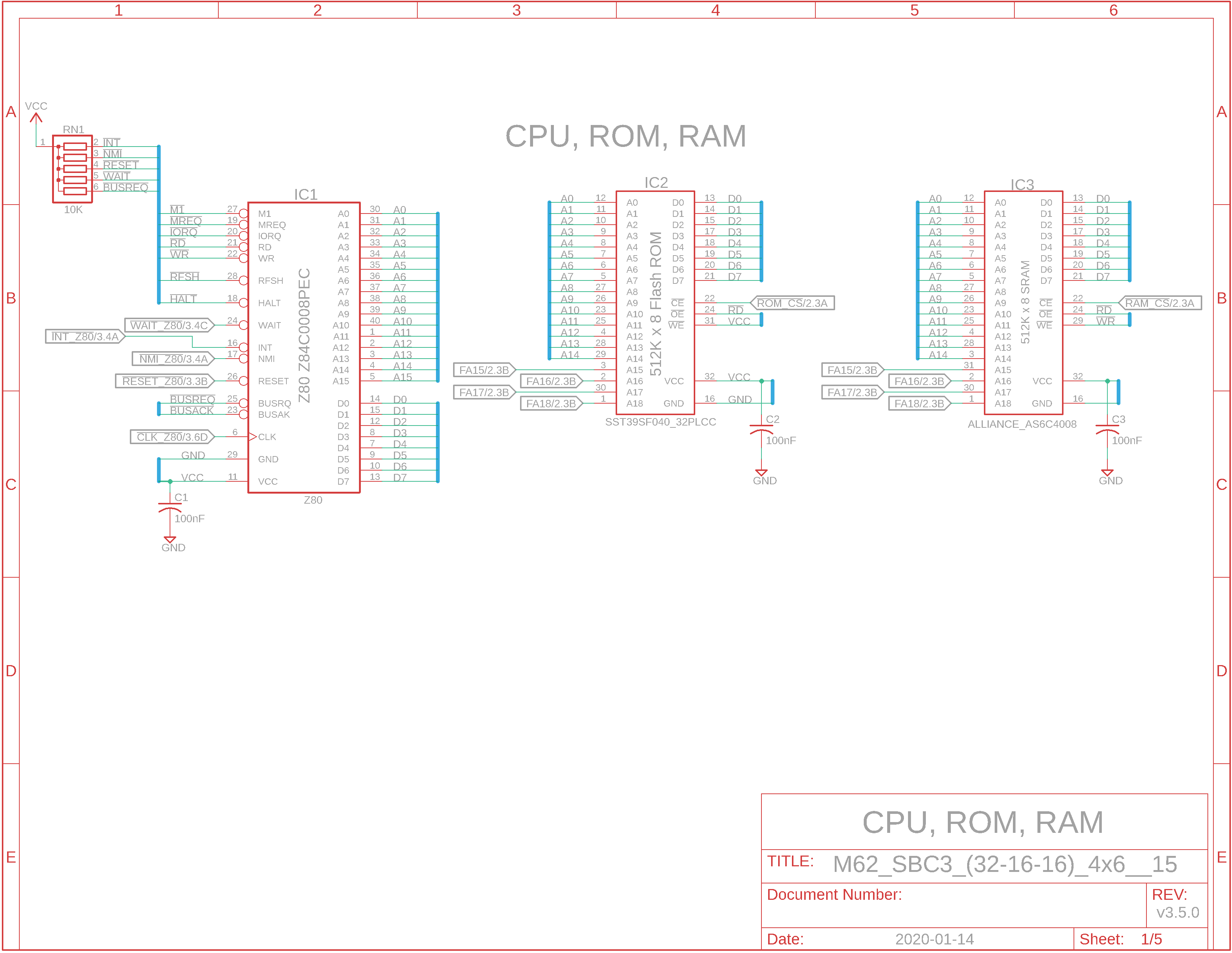
Eagle CAD: 1. CPU, ROM, RAM
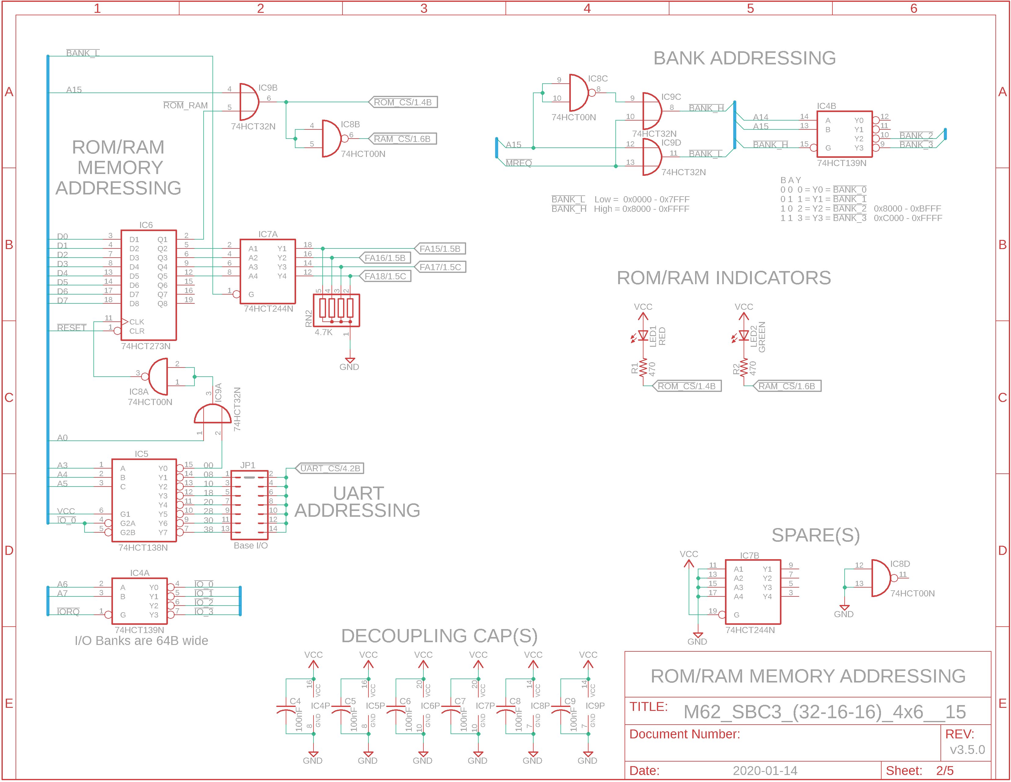
Eagle CAD: 2. Memory & UART Address Decode
Eagle CAD: 3. CPU Slow/Fast/Single-Step Clock
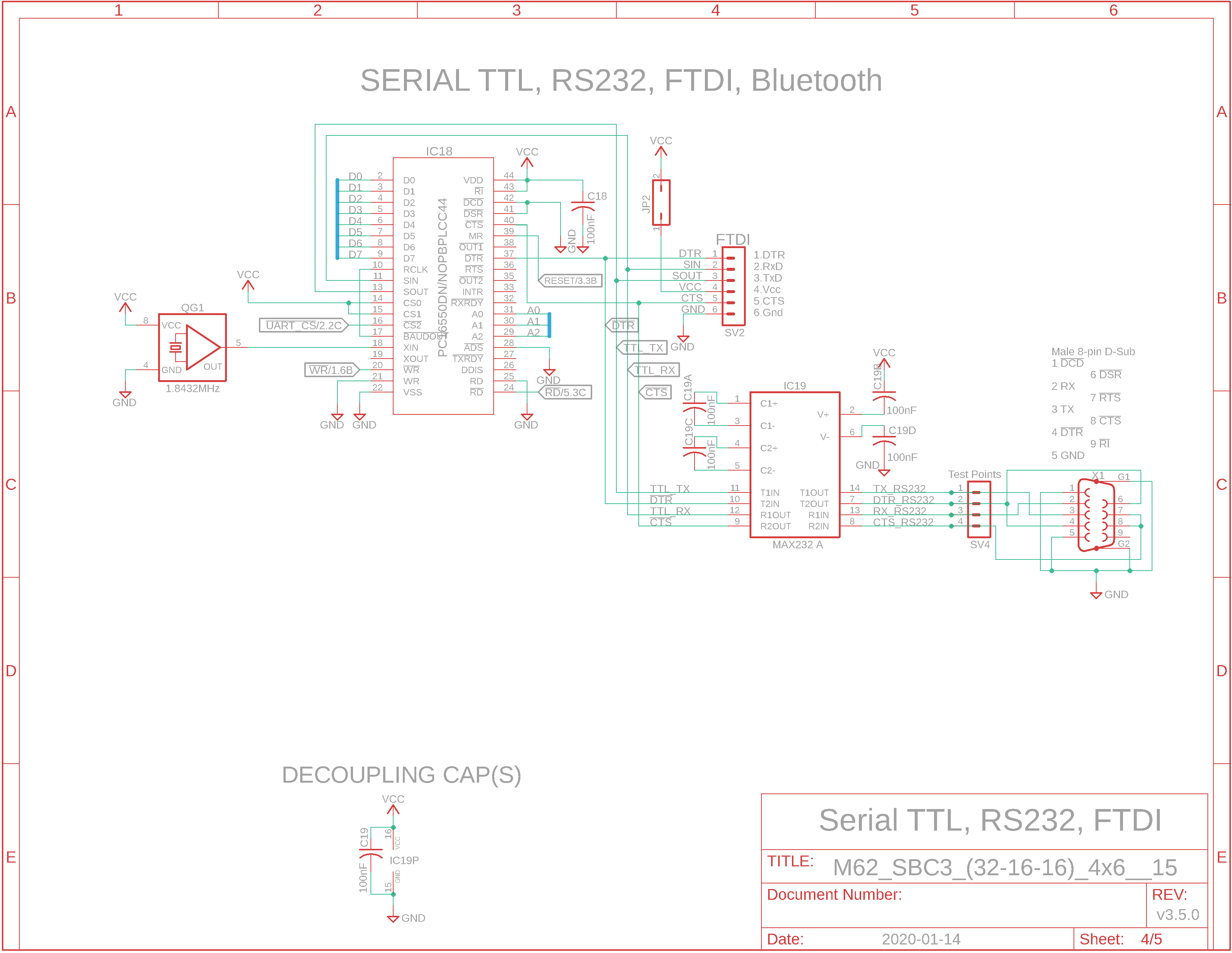
Eagle CAD: 4. UART, Serial FTDI, BT, RS232
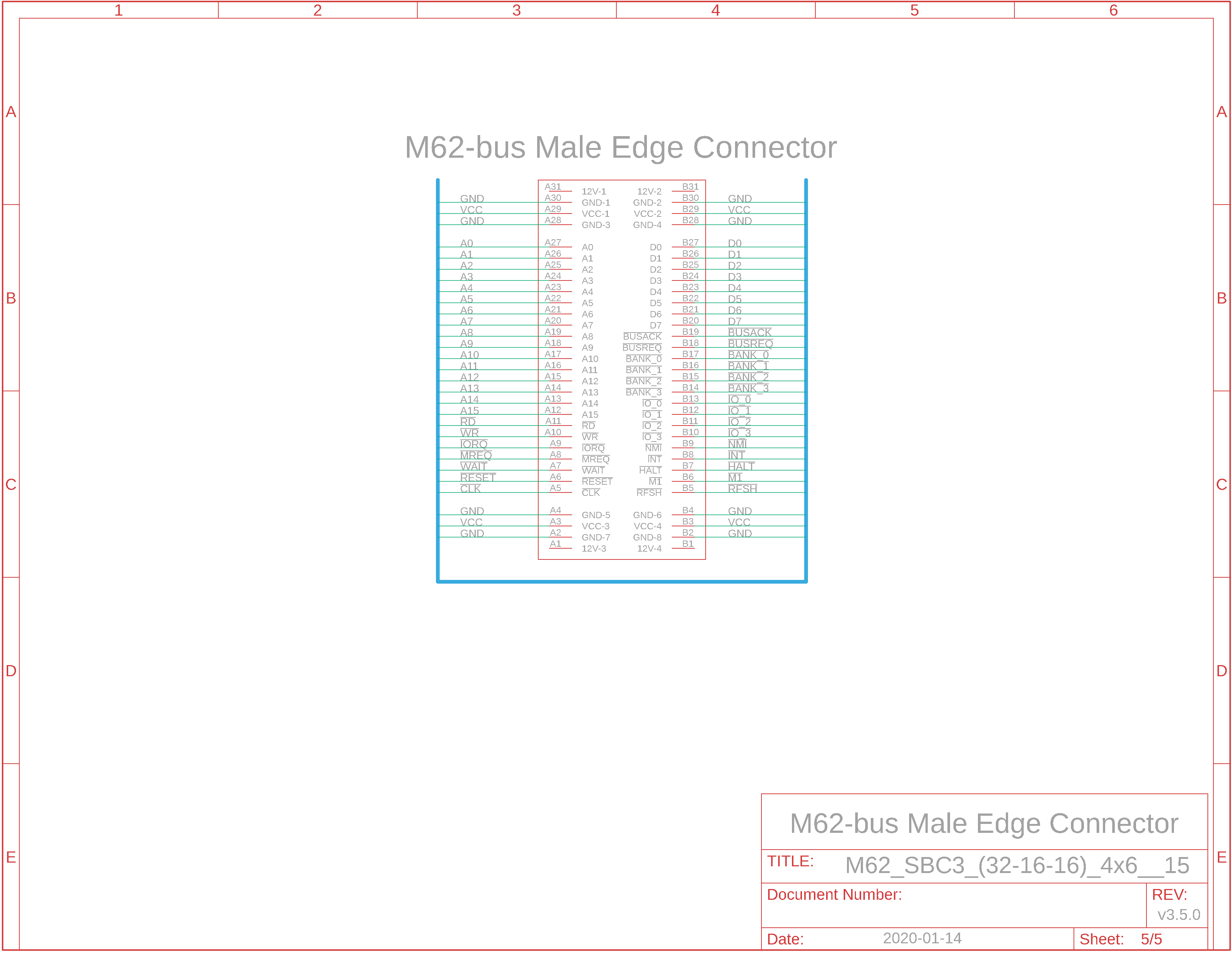
Eagle CAD: 5. M62-bus Male Edge Bd. Connector
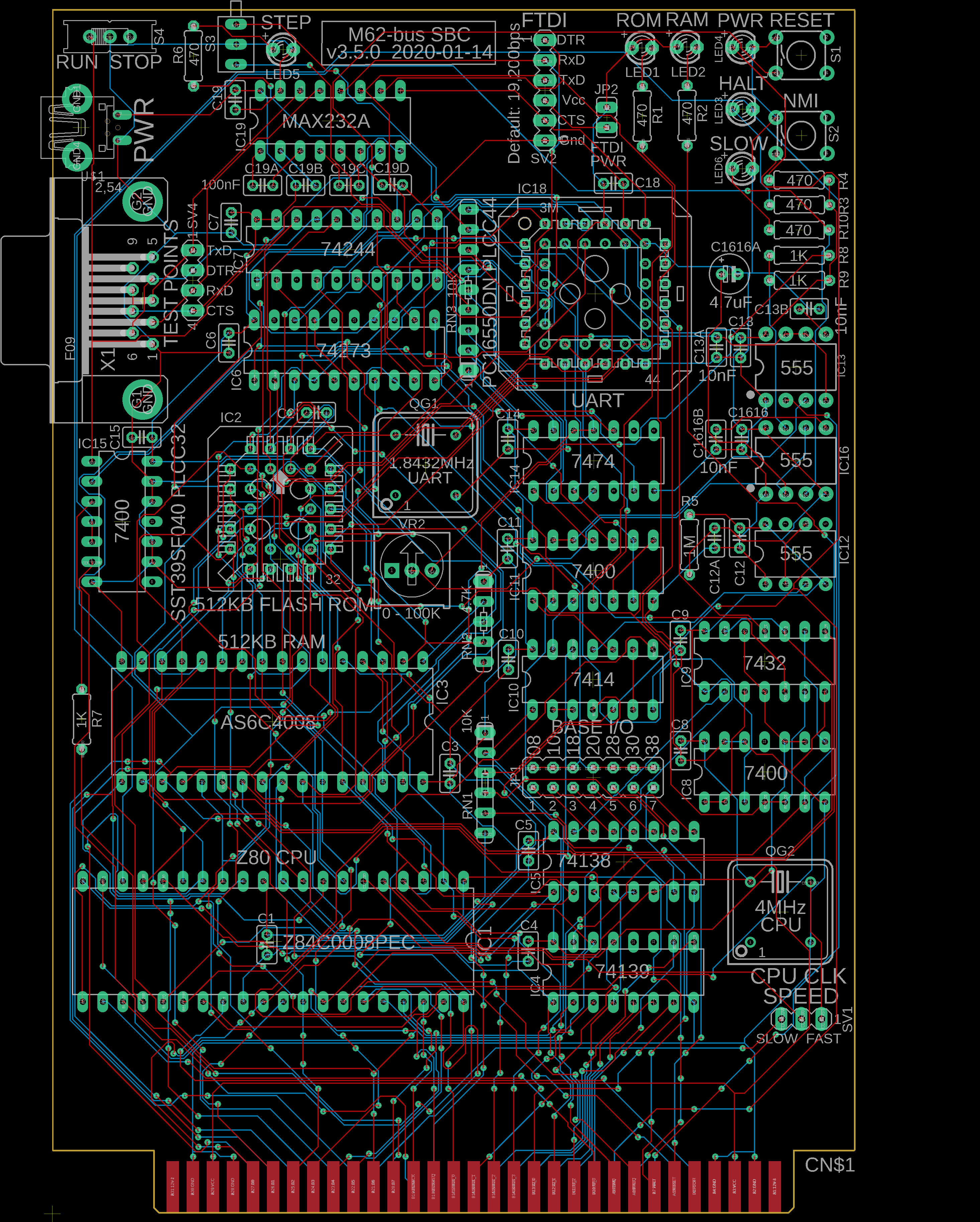
Eagle CAD: 6. Possible PCB Layout
(Bill of Materials)
|
PLEASE NOTE: I do not sell production boards. If you would like to buy an M62 Z80 system board/parts kit, contact Peter Murray, Peter@39k.ca I simply provide you with information to build your own breadboard computer.
NOTE: 2020-01-14 This board will be going out soon for fabrication. Use at your own risk until I have fully tested it.
This is the third version of the M62-bus Z80 single board computer, and it contains a few new requested features including ROM/RAM Bank Switching developed by Peter Murray
New Features 1) Slow-Fast CPU clock has been implemented. With a single jumper (SV1), you can switch between a fast (4MHz) CPU clock and a variable one that ranges from 1Hz to about 100Hz. This can be very helpful when testing new expansion hardware or code. 2) In addition to the CPU clock speed, single-stepping the CPU has been included. 3) This SBC uses two crystal oscillators: one for the CPU and one for the UART. As such, any comm speed up to 115,200bps is possible. BIOS v1.2.3 is defaulted to a speed of 19,200bps. If you wish to step it up, you'll need to modify line 24 of 16c550uart.asm before you assemble m62bios.asm. 4) The FTDI-USB connector SV2 is a right-angle female receptacle that points to the left side of the board. This is assumed to be the back of the rack/cage. You still have the choice of FTDI/USB or Bluetooth/USB, but not both at the same time. 5) Peter Murray of 39k.ca has devised a bank switching scheme to make more memory available onboard.
How much memory does SBC v3 have? 512KB ROM and 512KB RAM chips are installed (the chips are currently the market cheapest). Normally only a total of 64KB would be available to the Z80 CPU due to its 16-bit address bus and 8-bit data bus design. In SBC3, you have access to a total of 1MB with ROM & RAM switching.
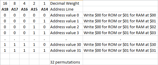
How does the bank switching work? You write $00 to the block you wish to use for ROM, $01 to the block you wish to use for RAM. If we write $00 to I/O $00, this will select ROM for Bank_0; this is the RESET default. If the ROM occupies 4KB of code, then the remaining 12KB of Bank_0 ROM goes unused. (Bank_0 to Bank_3 each contain 16KB of the system 64KB.) If we write $01 to I/O $00, this will select RAM for Bank_0 instead of ROM. That means we'll need to first copy the contents of ROM into Bank_1 RAM before we switch Bank_0 to RAM, then copy Bank_1 RAM to Bank_0 RAM. Our BIOS is at the same ROM location ($0000) as before but it's now in RAM. This frees up about 12KB of Bank_0 for RAM that would normally have not been available to our programs. In summary, when we write $00 to I/O $00 (ROM-RAM), this will select the 16KB block at position 0K as ROM; $01 at $00 for RAM. We can also address each FAxx address line (FA14 to FA18) as a 16KB block of ROM or RAM.
32 x 16K = 512KB RAM 32 x 16K = 512KB ROM That's a lot of memory!
How did we get here? You may have built the single board computer design using the following circuits from the Circuits Index page: - Z80 CPU Or you may be breadboarding using the up-to-date schematics in the left panel.
You will need to program the ROM with either the ROM Monitor or ROM BIOS v1.2.3 programs so you can communicate to the SBC via TeraTerm PC terminal emulation software.
What's next? You would probably like to produce or buy a PCB onto which you could solder sockets and parts. You could then transfer the breadboard ICs to the SBC PCB. Once completed and tested you would have your own working Z80 computer. The depopulated breadboards you used to build the SBC could be recycled to build your next project, maybe a flashy Bus Monitor Board or Console Board with VGA video and PS/2 keyboard connections?
How do I power my SBC? Via the mini-USB power plug or a powered backplane.
I want to build a number of the peripheral boards. How would I interconnect them to the SBC? How about an M62-bus powered multi-slot backplane?
I see the schematics. Where is the Bill of Materials parts list? The BOM is at the bottom of the adjacent panel.
How big is the SBC and what will the printed circuit board look like? The SBC PCB measures 100mm x 150mm (4"W x 6"H). Click on the adjacent thumbnail to see a possible parts layout.
Note: M62 Bus is copyrighted by Peter Murray of Murray Electronics, http://www.39k.ca |

![]()
Tags: Z80 SBC, 1MB memory