|
Build Your Own Z80: CIRCUITS I |
| Name | Circuit Schematics (click to enlarge) | Info | |||||||||||||||||||||||||
|
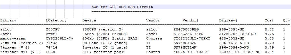
Z80 CPU
(Bill of Materials)
|
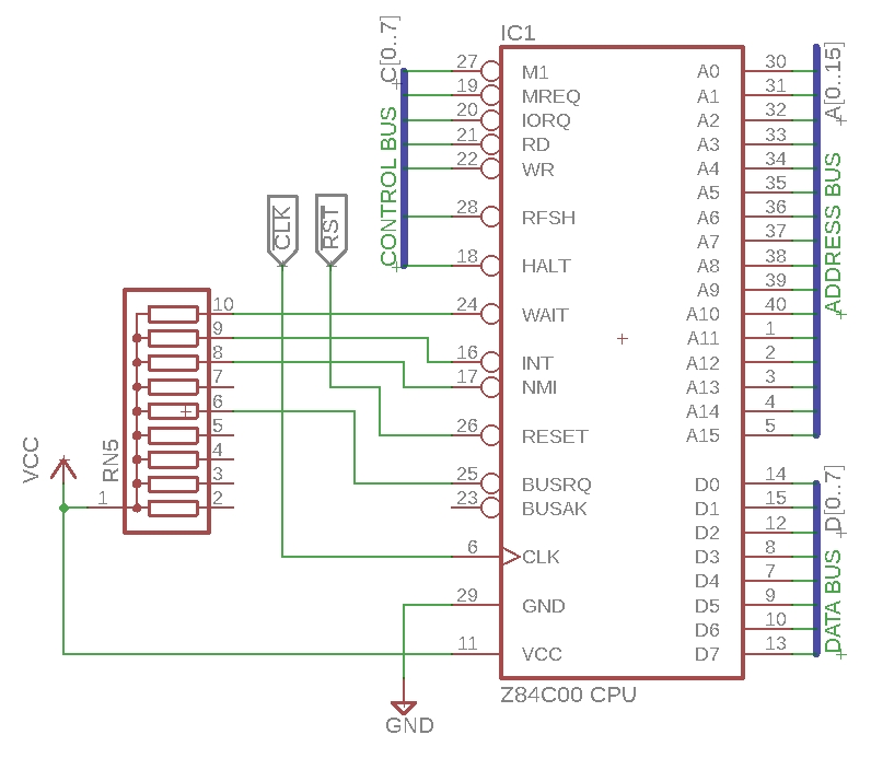
Eagle CAD: Z80 CPU Signals
|
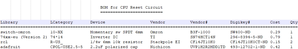
Terminating Unused CPU Signals All unused input signals to the Z80 should be terminated high: WAIT, INT, NMI, and BUSRQ. Consider using 10k resistors or a 10K resistor pack that is shown in the adjacent schematic. Signal RESET will have its own circuit that is normally a logic high (1) except during use. If you're using a slow clock (the CMOS version Z84C00xx can run from DC to its silkscreened speed), you will need to manually hold RESET low for 3 full clock cycles as per the Z80 spec. The CMOS version has the letter "C" in its part number. Example: Z84C0008 The NMOS version does not have that letter. Additionally, it can only run at its labeled speed, e.g. 4MHz If you're going to run the CPU NOP Test listed below, you really should use termination resistors to tie D0 to D7 to ground; 4.7k or a 4.7k resistor pack work well. We are not showing them in the diagram.
Test Your Circuit Visit CPU NOP Test to test your circuit. It contains useful info and a video demo.
Z80 Assembly Language Programming Visit Z80 Info VIII to learn how the Assembly code works for this circuit. |
|||||||||||||||||||||||||
|
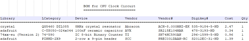
CPU Clock Frequency Divider
(Bill of Materials)
|
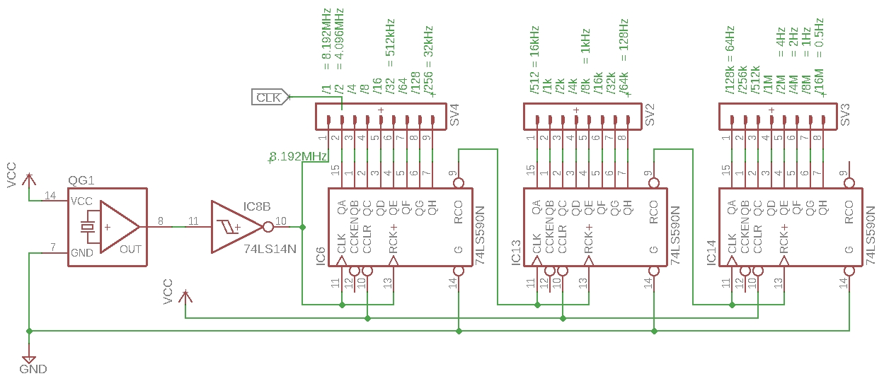
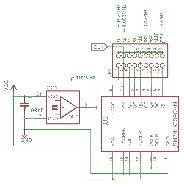
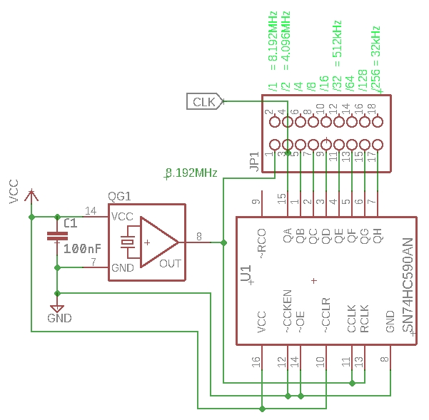
Eagle CAD: Clock Frequency Divider Eagle CAD: Clock Frequency Divider Simplified
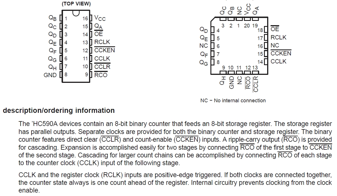
74hct590 8-bit Binary Counter
Digital Oscilloscope (DSO): 8MHz versus 1Hz Signals
|
This is not a true variable CPU clock because it uses numerically declining samples of the crystal oscillator frequency to provide CPU clock, i.e., 8MHz, 4MHz, 2MHz, etc. It will however meet most of our needs. In the adjacent top schematic, attached to the 8.192MHz crystal oscillator is a 74hc14 buffer/inverter that buffers the base crystal frequency of 8.192MHz before it goes into pin 11 of the first '590. (It's not really needed because the "can" oscillators have their own output buffering circuit.) Each output of the left-most '590 divides that signal by 2. At the last output, pin 7 of the first '590, the signal has been divided by 256 so it's now 32kHz. The Ripple Carry Out (RCO), pin 9 of the first '590, is attached to the Clock input pin 11 of the second '590. It's first output, pin 15, again divides the signal by 2 so it's 16kHz. The RCO of the second '590 is attached to the third '590 on pin 11, its Clock. Now its frequency is down to 64Hz. By the time we get to pin 7 it's only 0.5Hz so each CPU cycle is 2 seconds long. You will need a speed of about 500Hz for the 8255 I/O circuit and test. You will need a speed of 4MHz to test the LCD panel. If you have stability issues with your configuration, check to ensure CCLR is pulled high on all 3 devices. The CPU clock signal you may wish to use is simply wired/jumpered from one of the 8 possible '590 outputs to pin 6 of the Z80. Adjacent is a simplified version of the circuit with one '590 you will probably want to use.
|
|||||||||||||||||||||||||
|
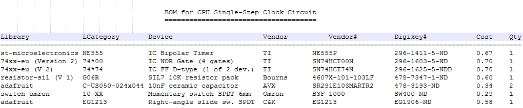
CPU Single/Multi-step Clock
(Bill of Materials)
|
Eagle CAD: Single/Multi-step CPU Clock
|
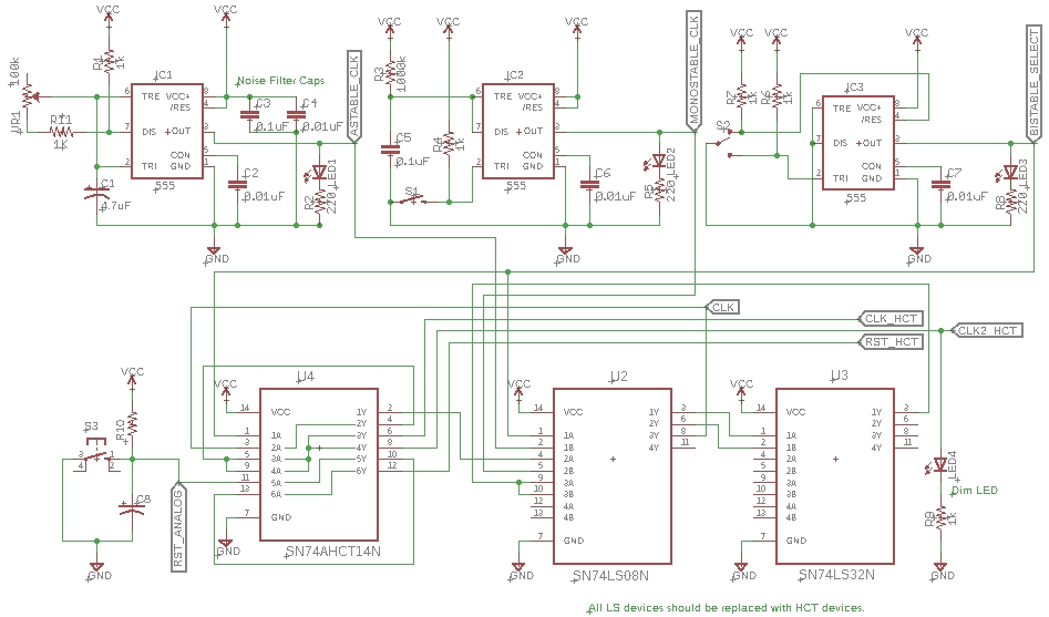
OPTIONAL: This CPU clock circuit contains both a multi-step circuit and a single-step circuit for the Z80. The CPU Reset circuit used in the "frame" below is included as part of the schematic. You can build the variable clock circuit using these four Ben Eater videos and parts list found here. Replace the LS devices with HCT devices if you`re connecting to the newer CMOS version of the Z80 CPU, Z84C00xx. There are two output signals, CLK_HCT and CLK2_HCT, the former you`ll connect to the Z80, and the latter is used to drive an activity LED because we don`t want to load down the CPU at all. |
|||||||||||||||||||||||||
|
CPU Single-Stepping Clock & Programming an EEPROM
(Bill of Materials)
|
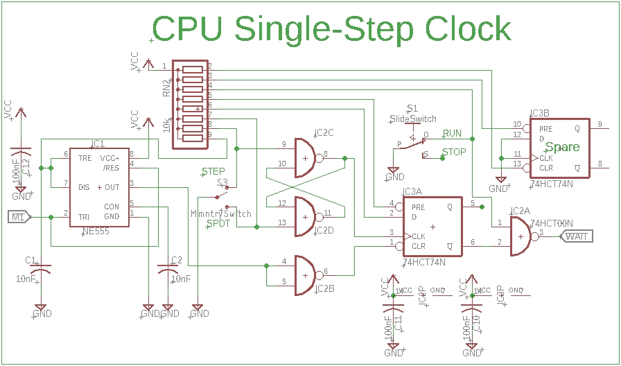
Eagle CAD: CPU Single-Stepping Clock
|
This CPU clock circuit uses the M1 and WAIT control signals (see page 5 of the Z80 manual) to single-step the CPU, and requires much fewer components than the Single/Multi-step circuit above. It's speed is determined by the RC circuit of the 555 timer and how fast you can press the Step button.
Note: M1 is only asserted at the beginning of an instruction, not for every byte operand that is to be read or written. Therefore, you will not see everything that transpires in your Z80 program.
We will test this circuit later once we have tested the ROM and RAM because we will be burning a small program to EEPROM that will copy a byte to contiguous memory.
Test Your Circuit Visit CPU Single-Step Clock Test to test your circuit. There is also a video on how to program your EEPROM for the test. |
|||||||||||||||||||||||||
|
CPU Reset
(Bill of Materials) |
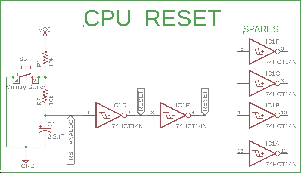
Eagle CAD: CPU Reset Circuit
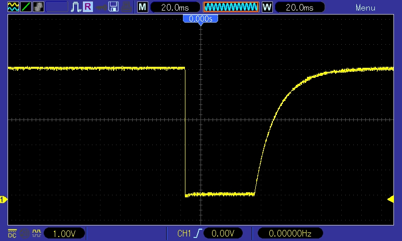
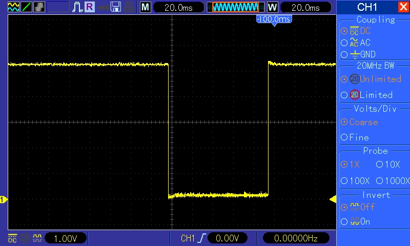
DSO: Analog CPU Reset Signal
DSO: Digital CPU Reset Signal
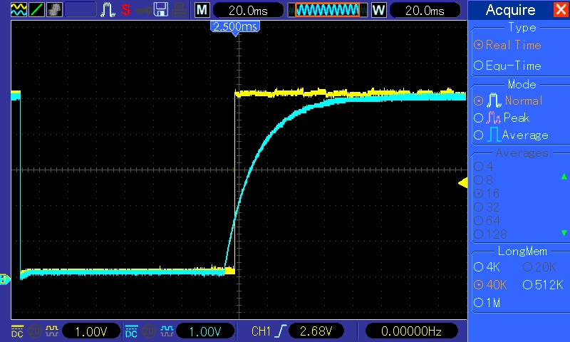
DSO: 2 channels of Analog and Digital
|
In the adjacent schematic, we see an analog reset circuit whose output
is fed to a digital IC. The upper oscilloscope screenshot below the
schematic
was taken where the signal feeds into the IC at RST_ANALOG,
and the middle o'scope screenshot was at the IC exit point called
RST_CPU.
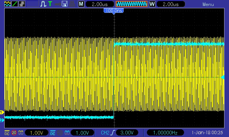
Once the 10K resistor and 2.2uF capacitor in series are fully charged, the signal is held high as "RST_ANALOG" to pin 1 of the 74hct14 inverter IC. The high signal is inverted on the output of pin 2 as a low which is fed back to pin 3 where it's inverted again to become a high on pin 4 as the "RESET" signal. Z80 RST is an active-low signal. The output from the inverter`s pin 4 is a logic high signal which is connected to pin 26 of the Z80. It will remain high until the momentary switch is depressed or the circuit is repowered. When switch S2 is pressed momentarily, it pulls the signal from the junction of the resistor/capacitor to ground. We can see that in the o'scope signal in the upper screenshot on the left (click it to enlarge the image). The signal is long enough (at least 3 CPU clock cycle times) to reset the Z80. The charge time for the RC circuit will be: 10K Ohms x 0.000 002 2 Farads = 0.022s or 22ms. If the CPU clock time is 6MHz, we expect the clock time to be: t = 1/f = 1/6,000,000 = 166us. 166 x 3 clock times = 0.5ms which is substantially less than 22ms so our minimum reset time has been met. Using the upper DSO screenshot, we can see the natural resistor-capacitor (RC) charge curve. The low, flat part of the signal illustrates the fastest time we could press and release the momentary switch. The curve to the right of the low, flat signal is the RC charge time. If the minimum input high voltage (VIH) is 2v, then we can see it took 3 dots of a 20ms/division display or 12ms of time to reach VIH . Again, this is substantially larger than 0.5ms for a 6MHz Z80 so our reset signal time frame is good. The fact that we are presenting the signal through an HCT version of an inverter, the 74HCT14, presents better compatibility with this older CPU. You can see the output of the 74HCT14 pin 12 to the CPU pin 26 in the middle screenshot. The third DSO screenshot was taken at a later date using 2 channels to contrast the analog reset to the digital reset of a 4MHz signal. TTL high/low reference. |
|||||||||||||||||||||||||
|
CPU Bus Monitor: Bar Graph LEDs
(Bill of Materials)
|
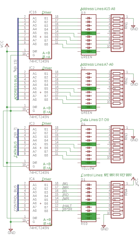
Eagle CAD: Signal Drivers and LED Bar Graphs
|
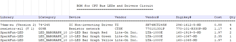
This circuit will display the address, data, and control lines to bar graph
LEDs. The adjacent schematic shows 74HCT245 drivers being used to drive the Bar Graph LEDs. The HCTs are a better match to the CMOS Z80 CPU (Z84C00xx) than LSs. Maximum Z80 CPU current drive varies with its posted speed. See below for specific values extracted from Zilog`s Z80 Z84C00xx CMOS Product Specification. If we assume 50mA maximum, every effort should be made to keep current requirements low. Connecting almost 30 LEDs to the address, data, and control bus lines with each requiring 10mA of current will easily exceed the limit and cause erratic CPU operation. Electrical Specifications: Page 34 of ps0178.pdf; earlier .pdf versions see page 30. Z80 CMOS version: 4.5v to 5.5v voltage supply. NMOS version: 4.75 to 5.25v. Output low voltage max: 0.4v Output high voltage min: 2.4v Input low voltage max: 0.8v Input high voltage min: 2.2v Z84C00xx CMOS CPU power supply current (max): 4MHz = 20mA, 6MHz = 30mA, 8MHz=40mA, 10MHz=50mA, 20MHz=100mA. Z8400xx NMOS CPU can handle 200mA of power supply current (see page 37 of ps0178.pdf), substantially more than the CMOS CPU. Unused low-active signals like NMI, BUSRQ, etc., should be tied high with pull-up resistors. Practical values range between 4.7K (1mA) and 10K (0.5mA). |
|||||||||||||||||||||||||
|
Memory: EEPROM & SRAM
(Bill of Materials)
|
Eagle CAD: ROM, RAM and Glue Logic
Addressing Logic
|
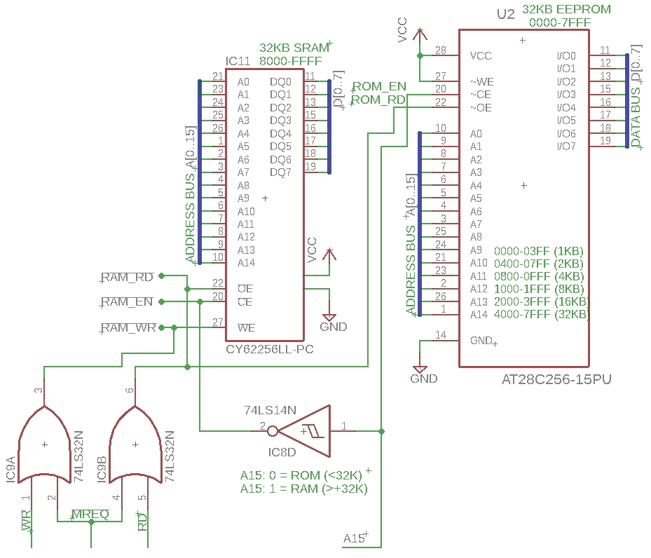
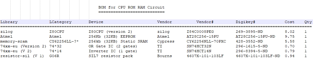
This circuit, via addressing "glue logic", will connect ROM (EEPROM) and RAM
(SRAM) to our Z80 CPU. The ROM will occupy the lower 32KB (0x0000 to 0x7FFF) and the RAM will occupy the upper 32KB (0x8000 to 0xFFFF) of our address space. Positive assertion of the A15 address line is for addresses of 0x8000 and above. As long as the addresses are below 0x8000, the EEPROM will be used (ROM_EN) because the 74HCT14 inverts the 0 signal on A15 to a 1, thus disabling the RAM_EN line to the SRAM. When address line A15 is asserted high, the RAM is used and the ROM is not. When both MREQ and RD are enabled during an M1 instruction fetch, either the ROM or RAM will be read depending upon the state of the A15 address line. Note that when MREQ is asserted, RD or WR is also asserted during the first byte read of the instruction. If the instruction is composed of multiple bytes, then an additional MREQ and RD/WR pairing is asserted for each byte. In our RAM test program listing, Block_Fill.lst, the first instruction is ``LD HL, 8000h`` which is composed of 3 bytes: 21 00 80. We expect the initial M1 and MR/RD, followed by two more MR/RD assertions. When both MREQ and WR are enabled during an M1 instruction fetch, only the RAM will be written to if A15 is high; this cannot happen if A15 is low because we tied the ROM`s WE line high to ensure the ROM contents are not accidentally changed.
Test Your Circuit Visit CPU EEPROM Test and CPU SRAM Test to test your circuits. They contain useful info and video demos.
Z80 Assembly Language Programming Visit Z80 Info IX to learn how the Assembly code works for this circuit. |
|||||||||||||||||||||||||
|
CPU Bus Monitor: 7-Segment LEDs
(Bill of Materials)
|
Eagle CAD: Z80 Bus Monitor
|
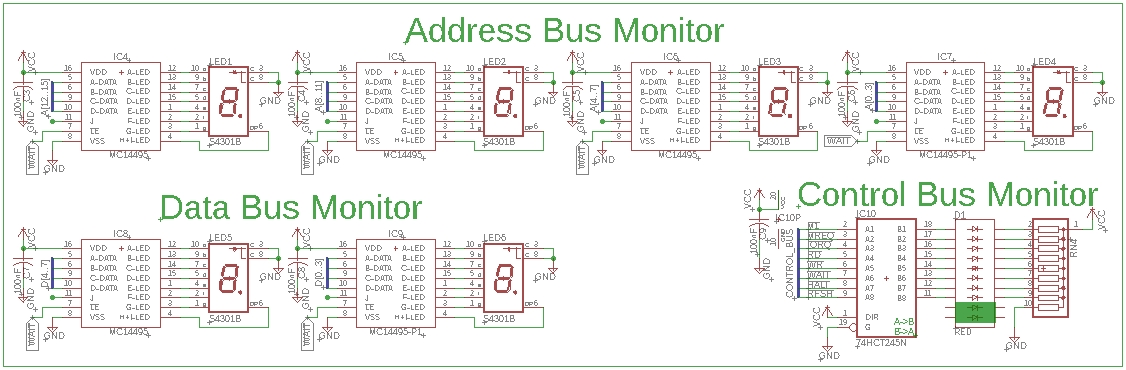
We could single-step the CPU with the earlier circuit using the bar graph LEDs but it would be more interesting if we built a circuit containing 7-segment LEDs for the Address and Data Buses; bar graph LEDs will be used for the control signals. We'll use the adjacent Z80 Bus Monitor circuit to view the code and signals as we step through the program.
Test Your Circuit Visit CPU Single-Step Clock Test to test your circuit. |
|||||||||||||||||||||||||
|
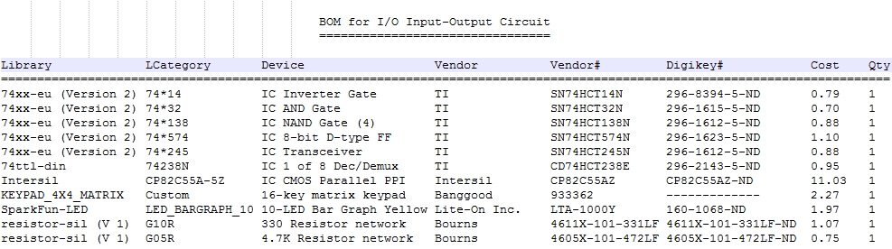
I/O: 8255 OUTPUT with LEDs
(Bill of Materials)
|
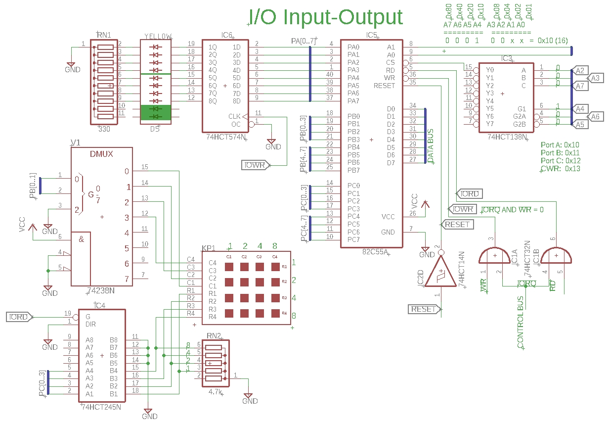
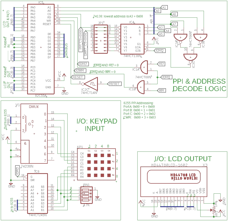
Eagle CAD: 8255 PPI and Display Logic
8255 Configuration Mode Definition Format for the Control Word
Register
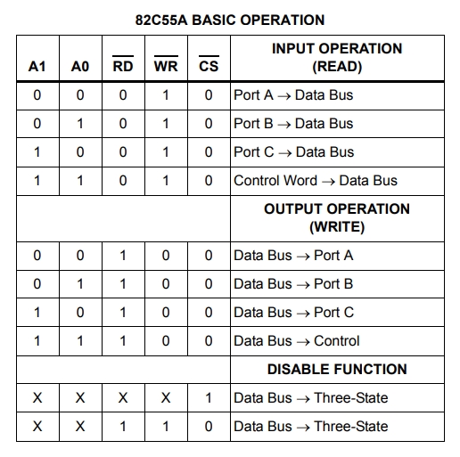
8255 Basic Operation
|
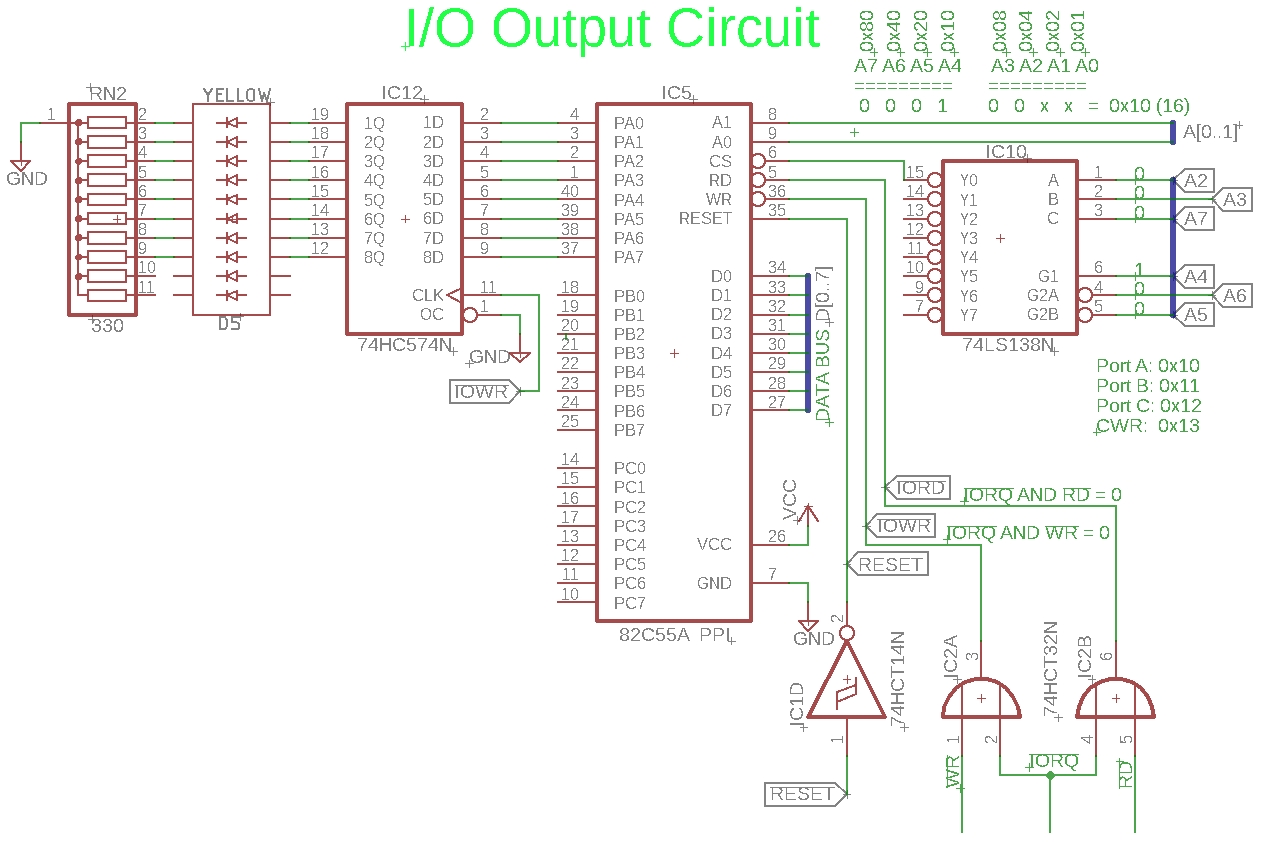
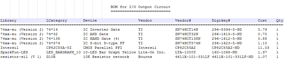
This circuit, via more addressing glue logic, will connect an 8255 Programmable Peripheral Interface (PPI) to our Z80 CPU. We will focus on the output aspect of this input/output (I/O) device. The output will drive bar graph LEDs.
The Z80 IN() and OUT() instructions use IR & RD or IR & WR, D0-D7, and A0 to A7. Generally speaking, they do not use the upper 8 bits of the Address Bus so there are only 256 possible IO addresses.
In the adjacent schematic, address line A4 connected to the '138 is the only line asserted positive. With A2, A3, and A4 low, output line Y0 will be selected if A5 and A6 are also low. Using A4 as a positive input to G1 to enable the '138 lets us select 0x10 as the starting address. If instead we chose A3 for G1 input, then the first address would be 0x08 up to 0x0B. If instead again, we chose A5 for G1 input, the first address would be 32 or 0x20; A6 would be 0x40; A7 would be 0x80. Looking at the binary weight table above the 74HCT138 3-line to 8-line Decoder in the adjacent schematic, we can see that usable addresses will begin with 0x10 (16 decimal).
The 8255 PPI (programmable peripheral interface) has only 4 user registers, hence the reason only A0 and A1 from the Address Bus are used: - Address binary 00 (address 0x10) is for Port A input/output (I/O) - Address binary 01 (address 0x11) is for Port B I/O - Address binary 10 (address 0x12) is for Port C I/O - Address binary 11 (address 0x13) is for the Control Word Register (CWR)
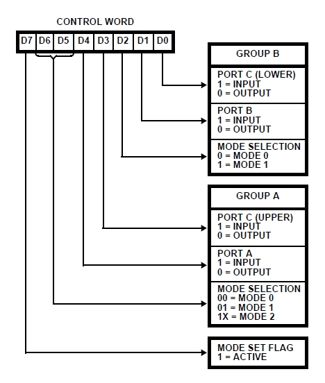
The CWR control word is shown adjacent. By setting the 8-bit byte to binary 1000 0000 (hex 0x80), we'll activate the 8255 and set all 3 ports as outputs in Mode 0 (basic input/output). We are using only Port A of the 8255 PPI. Once the 8255 device is addressed with 0x13 to set the control word of 0x80, we can send data on the Data Bus to address 0x10 for Port A.
The 74HCT574 is a latch that uses the IOWR signal (from the mating of WR and IR) to clock the data to the LED bar graph.
Test Your Circuit Visit Input/Output Test I to test your circuit. It contains useful info and a video demo. |
|||||||||||||||||||||||||
|
I/O: 8255 INPUT with 4x4 Keypad
(Bill of Materials)
|
Eagle CAD: 8255 PPI, 4x4 Keypad
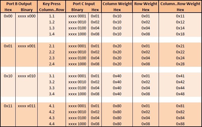
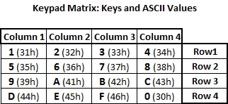
Column:Row Keypress Matrix
|
This circuit is a continuation of the last one. This time we will look at input with the 8255 using a 4x4 keypad.
A control word of 0x81 will set ports A and B as outputs and C as input. The idea is to drive a binary pattern out one port (B) and read what comes in on another (C); if the value is anything other than 0, then a key was pressed. The next step would be to determine which column and row, and then somehow display it to the user.
The '238 is a 3-line to 8-line non-inverting demultiplexer or demux. (A demultiplexer is a device that takes a single input line and routes it to one of several digital output lines.) If you present a binary value between 000 and 111, the output will be a 1 on the appropriate line. Examples: 000 yields a 1 on the 0 output (pin 15), and 011 puts a 1 on the 3 output (pin 12). Although the '238 has 3 inputs and 8 outputs, we will only use 2 inputs for 4 outputs to cover the 4 columns of the 4x4 matrix keypad. The idea is to send binary 00 out the 8255 on port B to the '238. The demux will output a 1 on the 0 output which is pin 15; this is the first column. Immediately after doing so, lower part of port C is read using IORD of the '245 pins 2 to 5 for the four rows. If the value read into the 8255 is binary 0000, then no key has been pressed. If the value is 1, we know the first row has been pressed, value 2 is second row, value 4 is third row, and value 8 is fourth row. In our example, if 00 (column 1) was sent and 0001 was received, the vector is column 1 and row 1. If 00 was sent and 1000 was received, the vector is column 1 and row 4. The adjacent matrix shows you all of the key press permutations.
The program we'll use for testing this circuit later is 4x4Keypad_WeightedColRow.asm. If 00 is sent and 0000 is received, no key was pressed. The program moves on to send 01 for the second column. If no key is pressed, 10 is sent. Again, if no key is pressed 11 is sent. By cycling through all four binary combinations on port B output for the four columns and reading the key press input on lower port C for the rows, we can "vector" the column and row pressed.
Now, how do we show the user which key was pressed? We can use 8 LEDs such that the left-most ones represent the column and the right-most ones represent the row. When the vector indicates column 0, then the row value of 1, 2, 4 or 8 is displayed as a binary value on the row LEDs. But we need to indicate the column value, too, so if we use the binary weighting of an 8-bit value, we can light up the corresponding LEDs.
Column Row 8 4 2 1 8 4 2 1 are the binary weights for column and row, left to right, respectively. 0 0 0 1 0 0 0 0 would show the first column as being chosen so we add 0x10 to the row value. 0 0 0 1 0 0 0 1 indicates first column and first row. 0 0 1 0 0 0 0 0 Adding 0x20 to the row value gives us the second column. 0 0 1 0 0 1 0 0 0x24 indicates second column and third row. 1 0 0 0 1 0 0 0 0x88 indicates fourth column and fourth row. This is detailed in the adjacent screenshot, Column:Row Keypress Matrix. This is our feedback to the user.
The clock has to be set high enough (500Hz) that IORD will occur during the key press. Set the clock speed too low and the key press may be missed.
Test Your Circuit Visit Z80 IO Output Test II to test your circuit. It contains useful info and a video demo. |
|||||||||||||||||||||||||
|
I/O: 8255 OUTPUT with LCD panel
(Bill of Materials)
|
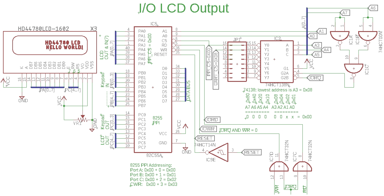
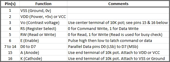
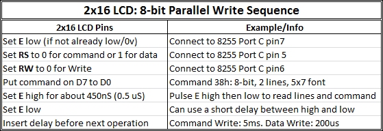
Eagle CAD: 8255, 2x16 LCD 2x16 LCD Pinout
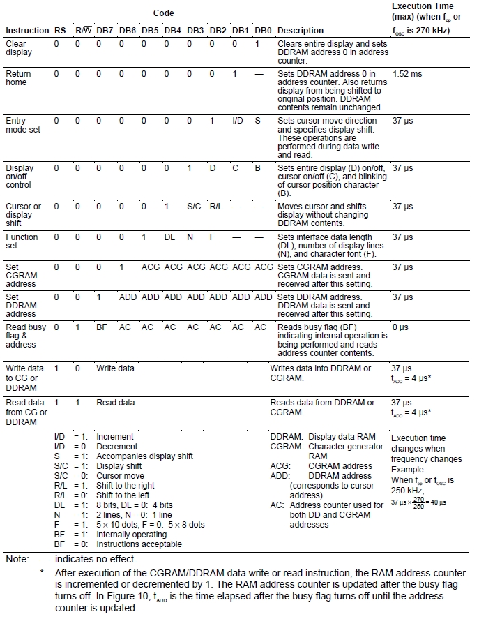
LCD Write Operation
LCD Configuration: Bit Definition Modes
|
In this circuit, we replaced the '574 and LED bar graph with a 2x16
(2 rows by 16 columns) parallel LCD panel.
The LCD can use 4-bit or 8-bit data lines; 4-bit means multiplexing the 4 data lines which makes the coding a little more complex. We have all 8 data lines available on 8255 port A so we'll use them for 8-bit mode. Adjacent is a schematic for the circuit that includes the LCD panel. The LCD Write Operation chart below the adjacent schematic shows the order of operation to output characters to the LCD. Essentially, it indicates the 3 control lines from the 8255 must be asserted before a control or data byte from the 8255 is sent to the LCD. To have the control lines and byte read/latched by the LCD, the LCD Enable line is pulsed high then low. We used Port B and Port C (low) for the keypad, so we have Port A and Port C (high) remaining for the LCD. Here's a summary of how we set up the keypad: - Port B output sends four binary combinations (00,01,10,11) to sequentially enable 4 keypad column lines. - Port C (low) input reads the four column rows to detect a key press when the circuit is made through the pull-down resistors. - If the key press occurs while outputting to column 1, the row read gives us the column/row vector, e.g., column 1 row 2 yields the vector C1R2 which was being sent to the LED bar graph for display. In the next Circuit we build, we'll send the vector to the LCD for display.
In this circuit we'll use Port C (high) for the control lines to the LCD and Port A to send display commands or display data to the LCD. The adjacent schematic shows the Port C (high) lines as PC[4..7]; we don't need pin 4, just 5 through 7.
Test Your Circuit Visit Z80 IO Output Test III to test your circuit. It contains useful info and a video demo. |
|||||||||||||||||||||||||
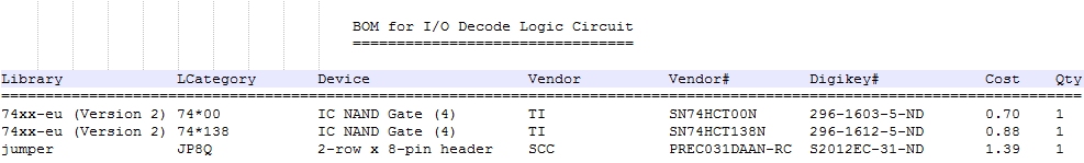
|
I/O Decode Logic
(Bill of Materials)
|
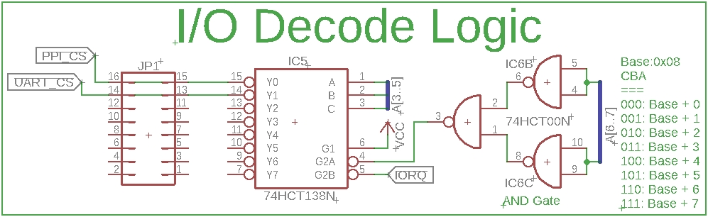
Eagle CAD: I/O Decode Logic
I/O Address Ranges
|
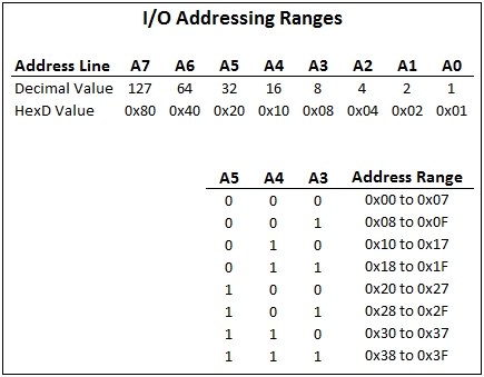
If you examine the decode logic used in the previous schematics above, you'll notice the address bus "feeds" to the 74138 decoder are not sequential. Moving forward in this and subsequent module designs, we're going to change the addressing so it is sequential. A0 to A2 will go to the device (PPI or UART) to convey commands or data, A3 to A5 are used for the addressed enable lines, and A6 to A7 are used to enable the '138 decoder itself at pin 4, G2A.
If I/O binary address 0000 0000 is chosen, the decoder is enabled on G2A and inputs A, B, and C. The first enable line output Y0 or pin 15 on the '138 is selected. This enables the PPI used for the keypad and LCD panel. Pins A0, A1, and A2 mean that eight I/O addresses (0x00 to 0x07) will be used to address the specific device; the PPI will only use A0 and A1, that is, addresses 0x00 to 0x03. Because the base address is 0x00, the addresses A0 to A2 addresses, 0x00 to 0x03, are added to the base address of 0x00 to create the final result of addresses 0x00 to 0x03.
If I/O binary address 0000 1000 is chosen, the decoder is enabled on G2A and the second enable line Y1 (pin 14) on the '138 is selected. This enables the UART used for serial FTDI or RS232 communications. Pins A0, A1, and A2 on the UART will be used, that is, addresses 0x00 to 0x07. Because the base address is now 0x08, the addresses 0x00 to 0x07 are added to 0x08 to create the final addresses of 0x08 to 0x0F. Consult the adjacent table, I/O Address Ranges for clarification.
If we need to add another device, the A4 address line will be 1 and the A3 line will be 0. A4 has a value of 16 or 0x10. Adding address 0x00 to 0x07 (from A0 to A2) to the base address of 0x10 will give us addresses 0x10 to 0x17.
For the next device, both the A3 and A4 lines will be used, thus the base address becomes 24 or 0x18. The full address range for that device will be 0x18 to 0x1F.
As you may have guessed, each addressable device will use a starting address that is a multiple of A3 which has a value of 0x08. |
|||||||||||||||||||||||||
|
IO: 8255 I/O with 4x4 Keypad and LCD Panel
(Bill of Materials)
|
Eagle CAD: 8255, 4x4 Keypad, 2x16 LCD
4x4 Keypad: Keys Matrix
LCD Instruction Codes
|
The three previous I/O circuits and tests have lead up to this one - input and output with an 8255 PPI. In this circuit, the keypad input and LCD output are merged together as Keypad-LCD-09_PPI-Address-00h_4.asm. Any key pressed will be displayed on the LCD panel in the left-most column.
Please note that we have changed the 74138 addressing wiring. You'll see it reflected in the adjacent schematic. This was necessary to make the addressing consistent for all I/O devices that would share the same 74138 3-line to 8-line decoder; alternatively we would have to add another '138 for each new device which is just a waste. (The 3 NAND gates in the upper right emulate an OR gate to ensure A3 through A7 are low to enable the 8255 PPI with I/O address 0x00.)
The first 93 lines of the .asm file are documentation indicating how the two devices are configured and used with the 8255 PPI. Lines 70 to 76 show the keypad keys matrix.
The adjacent Keys Matrix chart displays the ASCII codes each of the 16 keys (0 to 9, A to F) will send to the LCD for display.
The software uses a polling method, not an interrupt method, to read the key presses. That means pressing any key for more than a fraction of a second will cause multiple sequential displays of the same key - not quite what we want. The apparent fix is to send the LCD command 02h after any key press which "homes" the LCD cursor, effectively erasing the multiple displays of the same character.
When configuring the 8255, note that we will be using port C low and port C high, in addition to ports A and B. Port C low is the only input port.
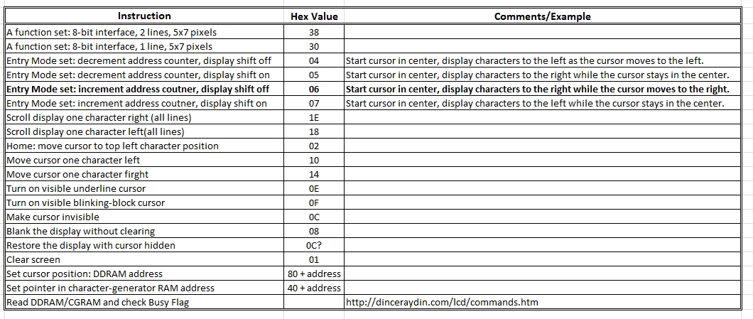
There are several commands listed in the adjacent LCD Instruction Codes chart as well as a simpler version found on the Test page as LCD Instructions. You may wish to experiment with them.
Test Your Circuit Visit Z80 IO Output Test IV to test your circuit. It contains useful info and a video demo.
|
![]()